Bruker Introduces OPTIMUS™ 2 Innovation for Improved Electron Backscatter Diffraction (EBSD) Characterization of Nanomaterials and Nanostructures
BERLIN, Germany – March 9th, 2021 – Today, Bruker introduces the OPTIMUS 2 detector head as part of a new “Augmented On-Axis Transmission Kikuchi Diffraction (TKD)” solution in Electron Backscatter Diffraction (EBSD). A comprehensive package of new hardware and software expands the EBSD applications range and improves the spatial resolution when characterizing nanomaterials and nanostructures in a Scanning Electron Microscope (SEM).
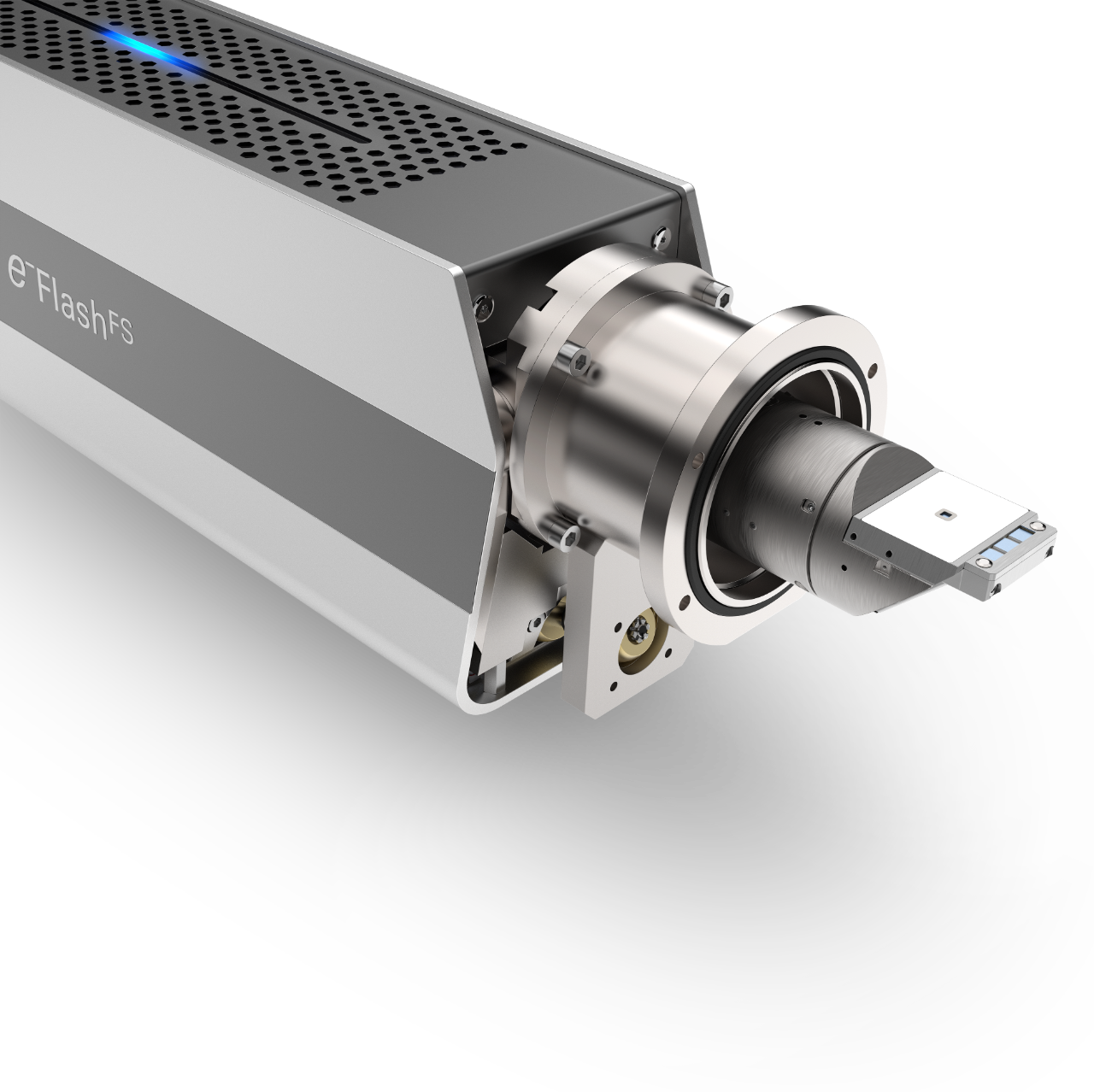
OPTIMUS 2 enhances Bruker’s eFlashTM EBSD detectors for crystal orientation mapping on electron transparent samples with even higher spatial resolution in SEMs. Its new STEM-in-SEM capability combined with new ESPRIT software features provides:
- new analytical capabilities for in-situ experiments
- superior data quality and data integrity
- improved user experience
- a boost in productivity for certain applications
Due to its unique design, OPTIMUS 2 improves spatial resolution to 1.5 nm and lower by optimizing beam focus and astigmatism settings before acquiring a TKD map. Moreover, OPTIMUS 2 for the first time enables the acquisition of orientation maps in the ultra-high resolution immersion lens mode in certain high-end SEMs. It reliably corrects pattern distortions induced by the strong magnetic field in the immersion lens by new, patent pending features in ESPRIT FIL-TKD (full immersion lens TKD) software.
ESPRIT TRM, another software feature of OPTIMUS 2, allows automatic time-resolved imaging and orientation mapping during dynamic experiments, like in-situ heating, electrical biasing and tensile testing. With OPTIMUS 2, high quality bright field (BF)-like images are acquired at up to 125,000 pixels/second for real-time visualization of electron transparent specimens during dynamic experiments.
Furthermore, high-contrast and high-resolution images produced by the new STEM-in-SEM imaging capability of OPTIMUS 2 can now be used to detect and compensate for beam and sample drift more accurately. This is particularly important when mapping nanomaterials where a beam or sample drift of just a few tens of nanometers causes visible artifacts.
BF-like images generated by OPTIMUS 2 can be binarized using ESPRIT MaxYield software applied as masks to efficiently map regions of interest on sparse samples, like nanoparticles or nanorods. To further enhance productivity, Bruker is also offering multiple TKD sample holder adapters that fit most SEM models and are made of advanced alloys to minimize drift due to thermal expansion.
Finally, the combination of OPTIMUS 2 with Bruker’s unique FlatQUAD EDS analyzer offers highly efficient simultaneous acquisition of structural and chemical information on the nanoscale.
“We are excited to announce OPTIMUS 2, which is the result of a collaboration with DTU Nanolab in Denmark,” commented Dr. Daniel Goran, Bruker’s Senior Product Manager EBSD. “With the new Augmented On-Axis TKD solution, we can make a significant contribution to the materials sciences by accelerating and improving the characterization of nanomaterials and nanostructures.”
Media contact:
Sandra Vodene
Head of Performance Marketing
Bruker Nano GmbH
T: +49 (30) 670990-0
E: sandra.vodene@bruker.com