Bruker
製品とソリューション アプリケーション サービス ニュースとイベント キャリア 企業情報
少なくとも2文字を使用してください (現在1文字を使用しています) 。

Languages

  • Deutsch
  • English
  • Español
  • Français
  • Italiano
  • Polski
  • Português
  • Русский
  • 中文
  • 日本語
  • 한국어
▶ Watch On-Demand | 1 Hr 28 Minutes

A Decade of Discovery Enabled by PeakForce Tapping

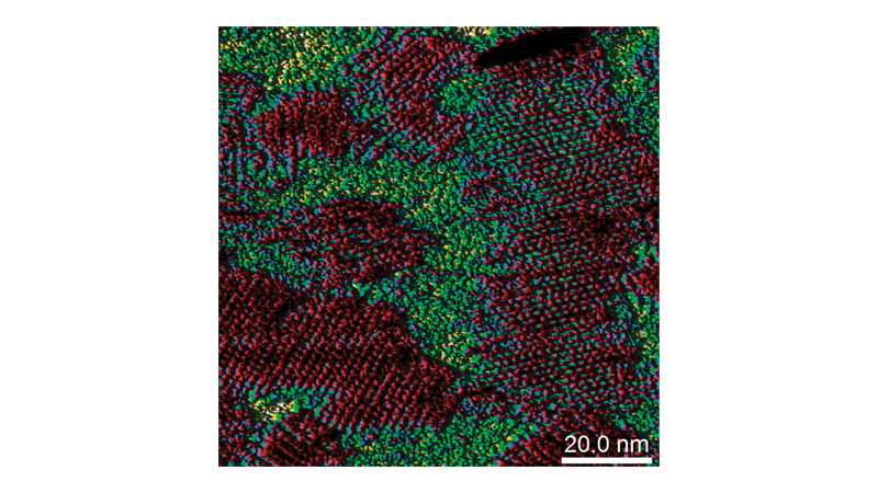
PeakForce Tapping has been widely adopted in a broad range of research fields, outpacing all other recently developed AFM modes in research impact and productivity.

このビデオを再生するには Cookie を受け入れる必要があります

Presented by Bede Pittenger, Ph.D. Sr. Staff Scientist, Bruker Nano Surfaces, AFM Applications, Bruker Nano Surfaces Inc., (April 22, 2020)

Featured Products and Technology

PeakForce Tapping Mode - Submolecular-resolution adhesion on iPMMA. 100 nm image. (Sample courtesy of T. Thurn-Albrecht, Martin-Luther-Universitaet Halle-Wittenberg)

PeakForce Tapping

Highest resolution imaging and property mapping
詳細はこちら
TR-Mode Teaser Image

Morphology Modes

Morphology modes are used to measure the nanoscale 3D structure of a surface.
詳細はこちら
Atomic Force Microscope Modes

AFM Modes

AFM modes and the broad capabilities from AFM beyond imaging
詳細はこちら
AFM-Materials-BRUKER

AFMs for Materials

Bruker's materials research atomic force microscopes, powered exclusively by PeakForce Tapping® technology, are helping researchers advance new nanomechanical, nanoelectrical, and nanoelectrochemical research, on the order of three peer-reviewed published articles per day.
詳細はこちら
AFM-PeakForce-Tapping-Poster-BRUKER

Free Download: PeakForce Tapping Poster

Download your 24x36 print-ready poster.
Download Poster
AFMi-EB103 The Definitive AFM Modes Handbook-BRUKER 1

E-Book: The Definitive AFM Modes Handbook

Everything you need to understand, select, and apply AFM techniques in materials research.
Download PDF
  • RETURN TO SESSION OVERVIEW
Bruker
© Copyright Bruker 2025
Imprint Terms of Use Privacy Notice Cookieに関する通知 Social Responsibility Reports