
Reverse Tip Sample (RTS) Scanning Probe Microscopy
Flipping the standard SPM tip-sample configuration
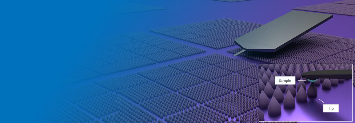
Reverse tip sample (RTS) scanning probe microscopy (SPM) was recently introduced by our guest speakers. RTS SPM overcomes the single-tip barrier of traditional SPM by flipping the conventional tip and sample positions, using a sample on a tipless cantilever and a vast tip array integrated into a nanofabricated probe chip.
Watch this on-demand webinar to hear about:
- Nanofabrication of probe chips
- Sample preparation
- Measurements and applications
Guest Speaker Abstract
We recently introduced the Reverse Tip Sample Scanning Probe Microscopy (RTS SPM) concept to overcome the single-tip barrier of the traditional SPM approach. This fresh perspective essentially flips the conventional tip-sample positions, placing the sample on a tipless cantilever and the tip on the sample stage, which is now a part of a vast tip array integrated into a nanofabricated probe chip. The standout feature of this arrangement is the ability to change tips seamlessly. During operations in RTS configuration the sample, mounted on the tipless cantilever, scans one of the thousands of tips present on the probe chip. When a tip wears out, the operator can quickly switch to a new one by just repositioning the cantilever onto an adjacent fresh tip, which takes merely seconds to complete. As such, the RTS configuration greatly boosts the data collection efficiency in application spaces where there is a need for frequent tip replacements and opens the door for further developments of the SPM technology.
After a comprehensive introduction of the RTS SPM concept, we also covered some of the crucial aspects mainly focusing on:
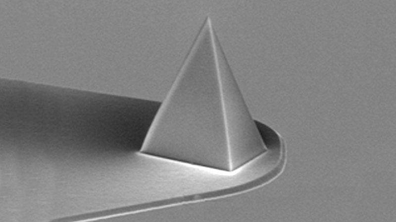
- Nanofabrication of probe chips: We presented a dry etching process for fabricating high-quality Si probe chips, which features a novel tip sharpening step. We also touch on the application of metal and diamond coatings on these Si probe chips.
- Sample preparation: We shared the dependable workflows we developed for routinely preparing RTS SPM samples by focused ion beam (FIB) and FIB-less approaches. These time-efficient procedures yield RTS samples with excellent electrical contacts and mechanical stability.
- Measurements and applications: We explored the diverse applications of RTS SPM such as statistical multi-tip studies, RTS Scalpel SPM, electrical tomography and more.
Find out more about the technology featured in this webinar or our other solutions for Scanning Probe Microscopy:
Featured Products and Technology
Speakers
Nemanja Peric, Ph.D., SPM Researcher, imec, Belgium
Nemanja Peric received his PhD degree from the University of Lille (France) while working at the Institut d’électronique de microélectronique et de nanotechnologie (IEMN/CNRS). After a short postdoctoral research period at IEMN, Nemanja joined imec in Leuven (Belgium) where he is currently working as an SPM researcher. His interests and expertise involve mainly AFM and STM.
Pieter Lagrain, Engineer, imec, Belgium
Pieter Lagrain received a master degree in chemistry from KU Leuven (Belgium). He joined afterwards imec as an engineer for nanoelectronics device analysis. His interest and expertise mainly involve FIB, TEM and SPM.


