
Automated AFM for Inline Hybrid Bonding Metrology in the Semiconductor Industry
Applying automated atomic force microscopy in inline metrology of hybrid bonding
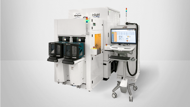
This on-demand webinar focuses on applying Automated Atomic Force Microscopy (AFM) in inline metrology of hybrid bonding in the semiconductor industry. Bruker’s fully automated AFM solutions enable the highly accurate, non-destructive, nanoscale characterization of surfaces, while delivering high-throughput data for inline process control and actionable data for hybrid bonding yield enhancement.
Webinar Summary
In this webinar, we illustrate how Automated AFM can be applied in the most current hybrid bonding technology nodes and wafer processing steps, and its suitability for labs and fabs working on new bonding device design. The following topics are discussed:
- Key Automated AFM features for process control in high volume manufacturing of bonded wafers
- High resolution imaging and analysis for critical bond pad metrology
- Large-area scanning of areas of up to 100s of mm2 for large scan topography in wafer-to-wafer bonding
- Automated bevel edge metrology for hybrid bonding
- Patterned and bare/blanket wafer defect review
Find out more about the technology featured in this webinar or our other solutions for inline metrology: