InSight WLI
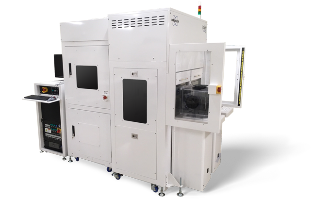
InSight WLI
InSight WLI is an inline 3D optical profilometry system built specifically for utmost metrology accuracy in high-throughput semiconductor manufacturing. It utilizes white light interferometry (WLI) to perform rapid, non-contact lateral CD and topography depth measurements with sub-angstrom precision and step-height capability into the hundreds of micrometers. Automation support includes SECS/GEM for 200 mm and 300 mm wafers, optional Cognex pattern recognition, and 35+ built-in analyses.
Specialized Inline Automation for Semiconductor Manufacturing
InSight WLI delivers fully automated, inline metrology with fast, consistent measurements and minimal operator intervention.
Core automation (factory + tool automation)
- Factory integration: SECS/GEM‑compatible automation for 200 mm and 300 mm wafers
- Tool automation: Recipe creation with autofocus and automatic tip/tilt to reduce manual setup
HVM‑focused workflow (inline flow + analytics)
- Inline wafer flow: EFEM handling with wafer ID reading and pre‑alignment for repeatable, production‑ready operation
- Production analytics: 35+ analyses and fast shape removal, auto hotspot detection, and database reporting with pass/fail criteria
Optional upgrades (automated targeting + enhanced detection)
- Pattern recognition: Cognex pattern recognition to support automated targeting and workflow consistency
- Advanced analysis: Vision64 Map™ for advanced visualization and enhanced defect detection/correlation
Benchmark for Accuracy and Robustness
High‑confidence 3D metrology enabled by white light interferometry
Because InSight WLI uses white light interferometry, it inherently delivers high‑precision, non‑contact 3D metrology that is not limited by field of view or working distance. Key advantages of WLI include:
- Vertical resolution: down to 0.01 nm; picometer-level accuracy
- Lateral resolution: down to 0.38 µm (Sparrow criterion); lateral resolution down to 200 nm
- Surface robustness: consistent results across translucent, reflective, and high-roughness features
- Confidence in results: robust repeatability across measurement modes
These features uniquely enable accurate, repeatable measurements across nanometer‑ to millimeter‑scale features, even on optically challenging semiconductor surfaces.

Interferometric advantages over other optical techniques
InSight WLI provides higher, more consistent vertical resolution than standard non-interferometric optical profilers, while improving throughput and measurement coverage in a single platform.
Compared to other optical and scanned optical beam technologies, InSight WLI uniquely delivers:
- Full-field topography: calculates height independently for each pixel across the full field of view, reducing time to results vs scanned optical beam approaches
- Transparent layer handling: segregates interfaces on transparent layers up to 100 nm
- One head, multiple tasks: covers a wide application range with a single optical head and transitions between measurement modes

Coverage Across Semiconductor Process Steps
InSight WLI supports FEOL, BEOL, advanced packaging, and MEMS metrology with non-destructive measurement and built-in analysis. Applications include:
- TSV/TGV monitoring
- CD monitoring
- Overlay monitoring
- CMP monitoring
- Die flatness qualification
- Edge inspection (e.g., ERO)
- Bump analysis
- Etch/deposition monitoring

How Can We Help?

Bruker partners with our customers to solve real-world application issues. We develop next-generation technologies and help customers select the right system and accessories. This partnership continues through training and extended service, long after the tools are sold.
Our highly trained team of support engineers, application scientists and subject-matter experts are wholly dedicated to maximizing your productivity with system service and upgrades, as well as application support and training.