InSight WLI
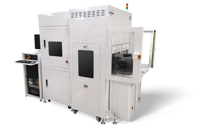
InSight WLI 搭载300mm晶圆处理系统
全自动的 InSight WLI 系统结合了卓越的光学表面测量功能与先进的晶圆处理系统,为用户提供前所未有的测量体验。该系统专为满足最为严苛的研发(R&D)、质量保证及工艺质量控制的需求而设计,搭载了专利性的探头倾斜设计(tip/tilt head)、独特的自校准激光参考( self-calibrating laser reference)、集成图案识别功能(pattern recognition)以及其他众多布鲁克独有的干涉测量技术。相比于其他量测系统, InSight WLI在非接触精度、高通量能力和操作便捷性方面遥遥领先,它能够广泛应用于各种在线生产量测和成像任务中。选择 InSight WLI,助力您在竞争激烈的市场中保持领先地位。
Specialized Inline Automation for Semiconductor Manufacturing
InSight WLI delivers fully automated, inline metrology with fast, consistent measurements and minimal operator intervention.
Core automation (factory + tool automation)
- Factory integration: SECS/GEM‑compatible automation for 200 mm and 300 mm wafers
- Tool automation: Recipe creation with autofocus and automatic tip/tilt to reduce manual setup
HVM‑focused workflow (inline flow + analytics)
- Inline wafer flow: EFEM handling with wafer ID reading and pre‑alignment for repeatable, production‑ready operation
- Production analytics: 35+ analyses and fast shape removal, auto hotspot detection, and database reporting with pass/fail criteria
Optional upgrades (automated targeting + enhanced detection)
- Pattern recognition: Cognex pattern recognition to support automated targeting and workflow consistency
- Advanced analysis: Vision64 Map™ for advanced visualization and enhanced defect detection/correlation
准确性和稳定性的标杆
InSight WLI 在准确性和稳定性方面树立了新的行业标准,这得益于其多项创新技术:
- 独特的测量传感器设计与专利性的双LED光源设计。
自校准、专为优化量测的激光参考源。
集成有减震功能的地装式机柜。

Interferometric advantages over other optical techniques
InSight WLI provides higher, more consistent vertical resolution than standard non-interferometric optical profilers, while improving throughput and measurement coverage in a single platform.
Compared to other optical and scanned optical beam technologies, InSight WLI uniquely delivers:
- Full-field topography: calculates height independently for each pixel across the full field of view, reducing time to results vs scanned optical beam approaches
- Transparent layer handling: segregates interfaces on transparent layers up to 100 nm
- One head, multiple tasks: covers a wide application range with a single optical head and transitions between measurement modes

满足产线严苛需求的配置
Configurations for Demanding Advanced Packaging
- Complete die flatness and CMP metrology solution
- TSV and interconnect measurements
- Hot-spot and defect detection on full reticle die
Factory Automation Ready
- SECS/GEM
- S2/S8 Compliant
- FDC, DCOL available

Coverage Across Semiconductor Process Steps
InSight WLI supports FEOL, BEOL, advanced packaging, and MEMS metrology with non-destructive measurement and built-in analysis. Applications include:
- TSV/TGV monitoring
- CD monitoring
- Overlay monitoring
- CMP monitoring
- Die flatness qualification
- Edge inspection (e.g., ERO)
- Bump analysis
- Etch/deposition monitoring