What is an SPM?
The Basics of SPM
A scanning probe microscope (SPM) is an instrument used for studying surfaces at the nanoscale level. SPMs form images of surfaces using a physical probe that touches the surface of a sample to scan the surface and collect data, typically obtained as a two-dimensional grid of data points and displayed as a computer image. The first SPM was the scanning tunneling microscope (STM) developed at the IBM Research Lab in Zurich by Gerd Binnig and Heinrich Rohrer in 1982. It was the first technology to be recognized as having atomic resolution capability.
An STM uses an electrical current between the microscope’s scanning tip and the sample to image the sample surface. Unfortunately, this means the surface of the sample must be conductive or semi-conductive, limiting the materials that can be studied. These limitations and others drove the invention of the first atomic force microscope (AFM).
Like most SPMs, the AFM uses a very sharp tip to probe and map the morphology of a surface. However, with an AFM there is no requirement for the sample to be conductive, nor is it necessary to measure a current between the tip and sample to produce an image. AFM employs the tip, or probe, at the end of a micro-fabricated cantilever with a low spring constant to measure the tip-sample forces as the tip presses (either continuously or intermittently) against the sample. Forces between the tip and the sample surface cause the cantilever to bend, or deflect, as the tip is scanned over the sample. The cantilever deflection is measured, and the measurements generate a map of surface topography.
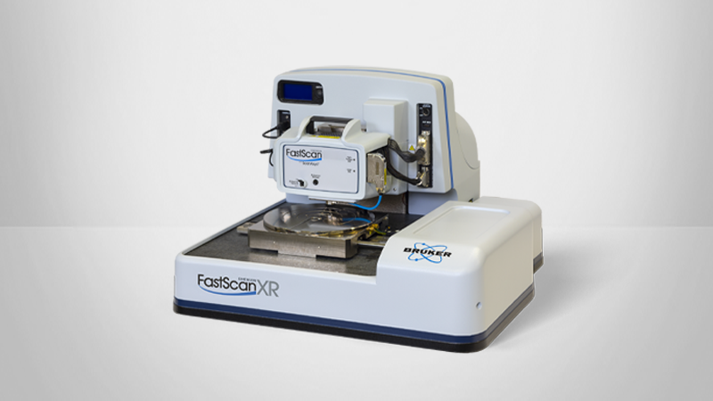
The evolution of SPMs has resulted in scientists and engineers being able to see structure and detail with unprecedented resolution, without the need for rigorous sample preps. Technical advances and the development of sophisticated techniques, or “modes,” have greatly extended the capabilities of SPMs, and particularly AFMs, across a wide range of research into materials and life sciences. Bruker is a world leader in AFM design, producing the most advanced atomic force microscopes and techniques, and our proprietary PeakForce Tapping® technologies give Bruker AFMs the widest array of application capabilities for measurement of nanoscale topography, and nano-mechanical, nano-electrical and nanoscale chemical mapping.