Wafer Level Packaging
Wafer Level Packaging
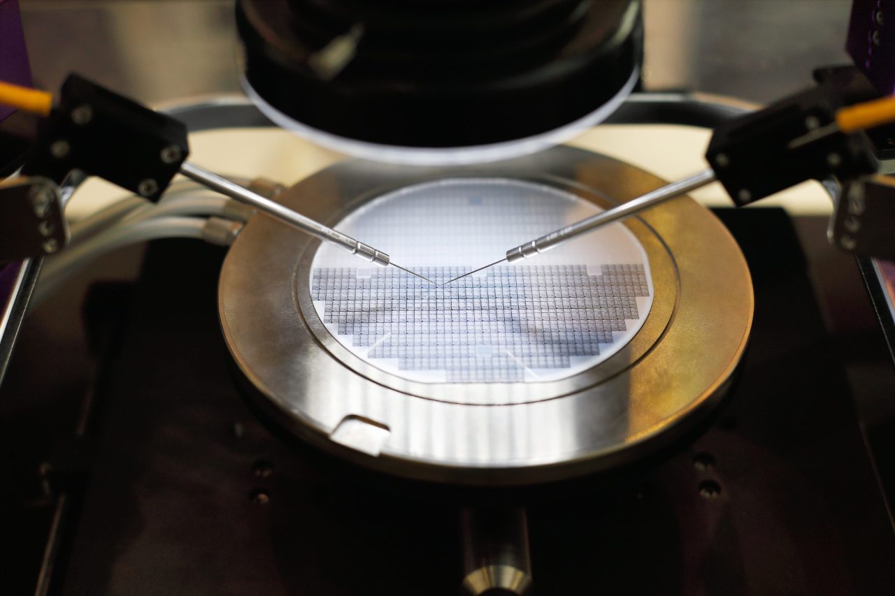
Bruker has a range of systems for wafer level packaging. Composition measurements on individual bumps and thickness of under-bump metals can be realized using micro-XRF.
RDL and Bumps
Semiconductor manufacturers face many key emerging trends in Wafer Level Packaging. These include:
- Redistribution Layers
- New UBM Films and Stacks
- Tighter Pitch Features
- Smaller Solder Balls
- Lead-Free Solder Alternatives
These critical trends create associated metrology challenges, and generate the need for:
- Thickness and composition control
- High sampling and high throughput
- Fewer blanket wafers
- Production wafer sampling
These needs drive the demand for non-destructive thickness measurements on RDL and UBM layers that include a small spot measurement technique with excellent spot placement, with tighter pitch densities (<200μm), and smaller solder balls (<100μm).
Other key considerations are composition measurements on the bulk UBM layer, where Ni(P) composition impacts the quality of the passivation layer, and composition measurements of lead-free solder alternatives:
- Sn/Ag composition → impacts reliability / prevents “shorts”
- Sn/Ag has shown to gain Ni or Cu from the UBM during the reflow process
XRF technology from Bruker answers these challenges via energy dispersive (~150eV) techniques with multi-detector array for fast, high-throughput measurements and 100% detector efficiency for Sn/Ag, plus small spot (poly-capillary) optics capable of measuring down to 50×50μm features. In addition, Jordan Valley XRF technology offers non-destructive real-time measurements that deliver immediate turn around.