Graphene and 2D Materials
With its ability to probe individual graphene flakes, providing nanoscale detail to the atomic level, atomic force microscopy has been part of graphene research since Geim and Novoselov’s Nobel prize winning discovery started the field. The early TappingMode images, acquired with a Bruker MultiMode® AFM at locations pinpointed by an optical survey, unambiguously identified the single graphene layers that had previously been thought to be inaccessible.
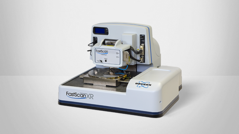
The years following this discovery have seen an explosion of graphene research activity, with well over 100 publications using Bruker AFMs. These studies include investigations into the fabrication of graphene and graphene oxide, where consistent product purity and known, low defect density are a key challenge, especially for scalable graphene production. They also address the wide ranging applications envisioned for graphene, from flexible displays and fast electronics to actuators, biosensors, and composites. Researchers at nearly every leading graphene research center are also using our Dimension XR, Dimension FastScan® and Dimension Icon® systems to drive their research in graphene and other 2D materials.

Advanced Property Measurements
Advanced property measurements have played a key role in the exciting AFM discoveries in graphene research. This research includes quantitative mechanical property mapping with Bruker’s exclusive PeakForce QNM® as utilized by Chu et al (J. Procedia Eng 36, 571 (2012) for unraveling graphene layering and by Lazar et al (J. ACS Nano ASAP 2013) for quantifying the graphene metal interactions controlling the electrode bonding in electrical device applications. Other examples are the nanoscale conductivity investigations on composites (Bhaskar et al., J. Power Sources 216, 169, 2012) and functionalized graphene (Felten et al., Small 9 (4), 631, 2013), as well as KPFM investigations clarifying the charge percolation pathway in optimized graphene oxide – organic hybrid FET devices (Liscio et al., J. Materials Chem 21, 2924, 2011).

Capabilities to Advance Future Research
The latest Bruker technology promises more exciting advances yet to come. PeakForce KPFM™ may permit extending the hybrid device investigations to higher spatial resolution, more quantitative measurements, and correlation with local material variations that could be revealed in simultaneous mechanical property mapping. Future conductivity studies may benefit from the proven ability of PeakForce TUNA™ to provide the highest spatial resolution on the most mechanically fragile samples. The investigation of defects in the 2D material graphene might be enriched by further PeakForce QNM studies, as this mode has been shown on 3D crystals to open the door to property mapping with atomic defect resolution.

2D Materials Data Gallery
Topographic map of graphene flake prepared on silicon dioxide, reveals expected 300pm graphene step between successive layers.

Graphene flake Raman G-band. Raman spectroscopy allows for fast mapping of graphene layer structure through G-band intensity.

The intensity of the D-band around 1350cm-1 indicates disorder of the graphene lattice. This D-band image suggests an area of increased defects along the edge of the single-layer portion of the sample.

The PeakForce KPFM image shows the single to bilayer graphene workfunction change to be 80mV, but then decreasing with each successive layer.

AFM topography image showing wrinkles in graphene layers at area of interest.

The detailed mechanical property measurements of the defect rich area reveal fine structures with greater compliance and reduced adhesion compared to the undisturbed portion of the layer, suggesting the graphene layer is wrinkled in this area.

The deformation channel shows a larger deformation on the graphene flake than on the substrate, and allows us to deduce that the graphene flake is softer than the silicon during loading, but does not mechanically relax during the sub-millisecond unloading.

This modulus image shows fine structures with greater compliance seen as darker areas on the modulus map image.