Performing Comprehensive Wafer Inspection with Non-Contact 3D Optical Profiling
Surface Inspection with Advanced Optical Profilers for Precision and Speed
3D optical profiling provides many advantages over other measurement techniques for non-contact inspection of semiconductor packaging front-end process research and control. These advantages range from fully automated measurements and non-destructive inspection to custom analyses and fast measurement speeds. Today’s most advanced optical profilers provide fast, accurate surface measurements to quantify a variety of properties about surfaces under inspection. These systems are used in engineering, research, and production process control around the world for an extremely wide range of markets, including precision machining, medical, microelectronics, MEMS, semiconductor, solar, data-storage, automotive, aerospace, and material science.
Contents include:
KEYWORDS: 3D Optical Profiler; 3D Surface Metrology; Profilometer; Application Note; White-Light Interferometry; Wafer Inspection; Semiconductor; Automation
Measurement Advantages of White Light Interferometry
3D optical profiling allows industry-leading measurement speed while maintaining the same nanometer Z accuracy at all optical magnifications. This combination enables the measurement of a very wide range of surface parameters, such as surface roughness, step heights, pitch, curvature, lateral displacement and waviness, all in a single measurement and on nearly any surface. The coherence scanning interferometry measurement technique, also known as white light interferometry or WLI (as detailed in Figure 1), can quickly determine three-dimensional surface shape and surface finish over large lateral areas, up to 8 millimeters in a single measurement, and vertical heights up to 10 millimeters. To measure even larger lateral surface areas, a stitching algorithm can be applied that allows multiple lateral images to be taken and stitched into one image for analysis. These capabilities have led to many metrology applications to meet the evolving wafer manufacturing needs.
3D Optical Metrology Analyses for Wafer Manufacturing
In general, wafer fabrication consists of sequential process steps to build components onto a silicon wafer, which eventually ends up as a complete functional device for a wide range of end products, from computer or memory chips to LEDs. As consumer electronics component sizes continue to decrease, there is a corresponding need for increased wafer metrology to refine and control the manufacturing of these complicated devices.
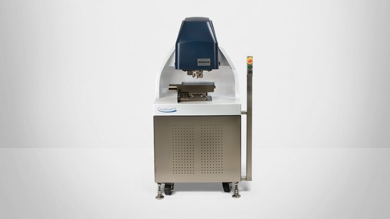
Below is a description of a few typical applications where 3D optical profiling is improving the manufacture and performance of wafers. All examples were performed with a ContourGT® 3D Optical Profiler utilizing Vision64® software (Bruker, San Jose, CA).
Trace Analysis
Most components designs utilize traces for electrical connectivity or device etching on the solid state device itself. Optical profiling can detect both vertical or horizontal lines and traces, as seen in Figure 3, where a Trace Analysis module automatically performed these measurements. The trace analysis was then able to report such parameters widths and heights for each trace, including the surface finish of traces and the spaces between them.
Multiple Region Analysis
Copper pillar, solder bumps, and through silicon via (TSV) are very critical manufacturing electrical and mechanical connections. A Multiple Region Analysis will automatically detect peaks, valleys, or levels from the terms removal reference plane (as seen in Figure 4). Once the regions of interest are automatically detected, different parameters of these features, such as surface finish, area, volume, height, depth, width, and pitch can be logged and controlled.
SureVision Analysis
Similar to multiple region analysis, a SureVision Analysis has the additional ability to pattern match to a feature in the field of view, align that feature or features to a template, then perform image masking, region modification, and analysis of up to 100 distinct regions in an image. This analysis option is very useful for under-bump metallization (UBM), which is commonly used for electrical or mechanical connection from the silicon die to a solder bump, as shown in Figure 5.
Subtract Images
Profilers with advanced software capability can subtract single or stitched images from within a wafer or from wafer to wafer. In this analysis, a reference image or stitched image is first captured, then subtracted from sequential measurements of a similar area. The subtraction software can remove pre-image waviness and form, align images run to run, and apply filtering as needed to the pre- and post-subtraction image. This is very helpful for monitoring height deviations from wafer to growing or lapping steps (as seen in Figure 6).
Thick and Thin Film Analysis
Films and coatings are necessary for insulation or isolation of key components within a device. Thick and Thin Film software can analyze metallic dielectrical films and coating material automatically. Film thickness can also be measured, depending on its index of refraction. The film software has the ability to detect modulation peaks on top and bottom of the coating to calculate the thickness of that film, as is shown in the theory example in Figure 7A.
Once the data is captured, the algorithm can report minimum and maximum thickness along with the surface finish of the top or bottom surfaces, as is shown in Figure 7B. In this example, the film analysis software can also calculate the uncoated pad height in reference to the base material under the coating.
Via Analyses
Advanced 3D optical systems also provide custom software algorithms for unique process analyses. Via Analysis finds the via and calculates a range of statistics, including depth, top and bottom diameters, and roughness of the anchor and via regions. A Glass Via Analysis calculates the via top and bottom diameter and depth, including the height of the glass fiber reinforcement layer using a special measurement mode algorithm. A Solder Resist Analysis finds a hole in the solder resist and calculates the thickness of the solder resist layer, top opening diameter, bottom diameter, and tail diameter and depth (as seen in Figure 8).
Overlay (Registration) Analysis
Basic and advanced Overlay (Registration) Analysis is used to analyze and characterize “feature-in-feature” geometries to track any relative shift of one surface with respect to the other surface, as seen for basic registry features analysis in Figure 9. More advanced registry and laser-inscribed features can also be analyzed simply by selecting the proper analysis checkbox required for the analysis.
Through Silicon Via (TSV) Measurements
For more challenging TSV measurements, certain measurement objective and field-of-view combinations can be used to measure the aspect ratios of “depth to width” of around 10 to 1. These TSV measurements are very important for wafer level packaging in improving areal density for stacked components (see Figure 10).
Measurement Automation and Wafer Handling
Advanced automation software is what often separates whether a system is truly useful for wafer manufacturing or not. Over the years, Bruker has worked with semi industry leaders to develop multiple stage-automation modes. XY Scatter mode allows the user to place multiple single-point measurement locations randomly throughout the wafer measurement area. XY Grid mode automatically creates a grid of known die size in a given XY pattern of columns and rows. Within each measurement grid die location, multiple measurements can be made (see Figure 11). Lastly, XY MultiGrid mode is similar to XY Grid, but the measurement grid die locations can be randomly placed around the wafer. In addition, XY MultiGrid has the ability to add fiducial alignment points for each measurement grid location while allowing each grid location to perform unique measurements from the other.
For each of the stage automations, a separate Vision recipe can be configured for each measurement location, including stitching multiple images together. Each of these measurement locations can also have a unique Z location that the profiler will automatically move to, significantly reducing measurement times. All automation types can also include alignment points that can be fully automated using Cognex pattern-matching capability. In addition to stage automation, Vision64 allows full automation of Autofocus, Auto Intensity, and Auto Tip/Tilt. Automatic feature centering in the field of view before measurement using pattern matching improves measurement robustness and repeatability.
Wafers can either be manually loaded onto the profiler stage for analysis, or can be configured with a wafer handler and environmental enclosure, as is shown in Figure 12. Not only does this enable unattended measurement of multiple wafers with integrated FOUP, but also to achieve class 2 type mini environments to meet all wafer manufacturing factory needs.
Conclusion
For wafer manufacturing, such as wafer-level packaging, flip-chip packaging, or TSV technology, an advanced 3D optical profiler can give engineers, process designers, researchers, and quality control professionals a significantly improved means of characterizing features for shape, surface finish, and overall functionality. 3D optical profilers are well established throughout a wide range of industries, from medical implants to aerospace components, and have been shown to outperform other measurement techniques in overall resolution, repeatability, accuracy, and speed. Bruker’s 3D optical profilers utilize industry-leading analysis and automation software, and are production-floor ready, providing a preferred metrology option for research, quality inspection, and process control. With dual-LED light sources and sophisticated algorithms, these systems are capable of making surface measurements with any reflectivity. Correlation to stylus measurement systems can be achieved with upfront knowledge of the surfaces being measured and the setup of the stylus tool. The addition of the 3D surface S parameters greatly extends the degree to which surface analysis can uniquely characterize surface shape and functionality. Bruker’s 3D optical profilers offer the most advanced improvement in measured data for the wafer industry.
Author
Roger Posusta, Senior Marketing Application Specialist, Bruker Nano Surfaces Division (roger.posusta@bruker.com)

