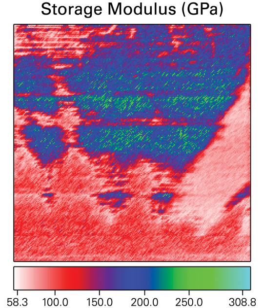
Modulus Mapping
High-Resolution Mechanical Property Imaging
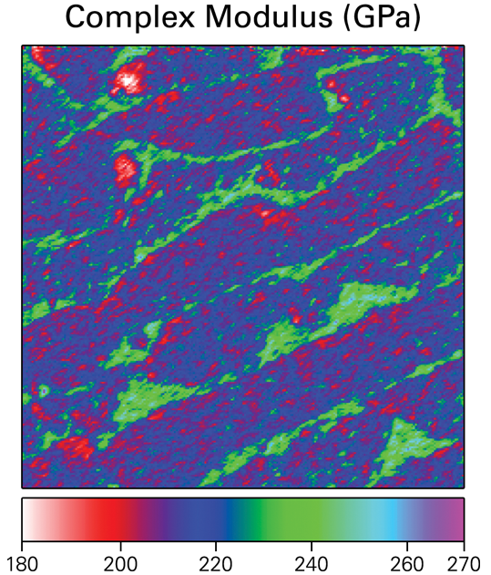
Bruker’s Modulus Mapping combines the powerful capabilities of Hysitron’s nanoscale dynamic analysis (nanoDMA III) with in-situ scanning probe microscopy (SPM) imaging to quantitatively map nanomechanical properties of a material’s surface. During a Modulus Mapping measurement, a rigid nanoindenter probe oscillates at a highly controlled force amplitude while being raster scanned over the sample surface in SPM imaging mode. The resulting displacement amplitude and phase lag are utilized to quantitatively measure viscoelastic surface properties. Each modulus map is comprised of 65,536 individual tests that can be performed in as little as ten minutes. Modulus Mapping is ideally suited for high-resolution mapping of inhomogeneous surfaces and interfaces.
Elastic and Viscoelastic Property Characterization
Modulus Mapping raster scans the indenter probe over the sample surface with a small oscillatory force while monitoring the resultant displacement and phase lag due to material response. A single scan of an area provides topographic information, stiffness, storage and loss modulus, and tan delta maps. This micron-area characterization technique provides the information necessary to guide the researcher to areas that may require further investigation of nanoDMA, such as single-point frequency or load sweeps.