
Semiconductor 3D Metrology Using Stylus Profilers
Improve device performance and manufacturing processes.
In this two-part webinar, Bruker profilometry experts discuss and demonstrate how Dektak stylus profilers deliver precise, repeatable surface measurements critical to semiconductor device performance and process control.
Viewers will
- Gain a practical understanding of stylus profilometry — including system architecture, hardware innovations, and strengths when measuring a range of diverse and increasingly complex materials and structures. Sessions highlight key semiconductor applications such as step height measurement, etch process monitoring, wafer curvature analysis, and stress mapping.
- See how the system delivers high-quality results on complex topographies and transparent films, helping to ensure process stability, dimensional accuracy, and consistent device yield.
Both parts feature real-time demonstrations of Bruker stylus profilometry hardware and software, showcasing real-world measurements and workflows from measurement setup through data analysis.
This webinar is included in our Thin Film Characterization Knowledge Pack.
Webinar Summary
Part 1: Leveraging stylus profilometry for semiconductor research and manufacturing
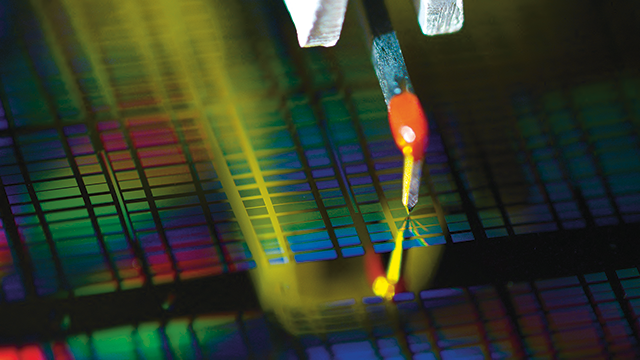
Stylus profiling is a precise surface measurement technique widely used in semiconductor research and manufacturing. It offers sub-nanometer vertical resolution and consistent repeatability, even on complex topographies and transparent thin films. This method supports a variety of process and quality control applications, providing reliable data that helps ensure accuracy and consistency in increasingly advanced device architectures.
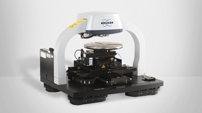
This webinar begins by reviewing stylus profilometry fundamentals, focusing on system architecture and hardware innovations, before discussing and demonstrating key applications.
Key applications explored in this webinar include step height analysis, wafer bow and curvature measurements, and stress calculations. It also includes a live demonstration using Vision64 software to showcase system setup, automation, and quantitative output capabilities.
This presentation is also included in Surface Characterization of Semiconductors: An Overview, from Topography to Advanced Physical Properties
FEATURED PRODUCTS AND TECHNOLOGY:
Part 2: Stylus profiling for high vertical resolution and long-range flatness measurements
Bruker’s Dektak stylus profilers capture nanoscale surface variations with high precision and accuracy — regardless of scan length and the optical properties of the surface. This enables repeatable, high-quality measurement on a broad range of materials and structures, even during long-range scans. These capabilities are critical for ensuring accurate and consistent surface metrology for both semiconductor research and manufacturing applications.
Watch this webinar to hear about the capabilities and advantages of using stylus profilometry and its impact on device performance and yield. Applications discussed include:
Join us for this webinar to hear about how stylus profilers are used for:
- Step height measurements
- Etch process control
- Wafer curvature analysis
- Stress mapping
The recording includes a live demo of the Dektak system in action, showcasing how step height measurements are performed across varied geometries. Viewers will also see how Bruker’s Vision64 software streamlines the workflow — from setting up measurements to analyzing and interpreting results — making it easier to integrate high-precision metrology into day-to-day operations.
This presentation is also included in our Surface Characterization of Semiconductors Workshop
FEATURED PRODUCTS AND TECHNOLOGY: