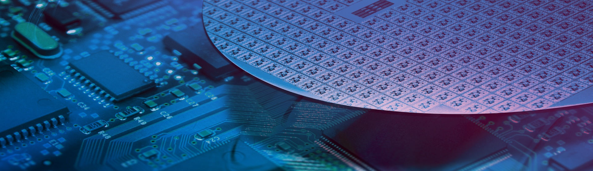

Surface Characterization of Semiconductors: An Overview, from Topography to Advanced Physical Properties
Discover the most impactful innovations in semiconductor research.
This presentation focuses on Bruker’s solutions for nanometer-scale surface characterization of semiconductor materials and devices and the common questions and challenges facing scientists in this field. See real-time demonstrations of Bruker technology and the latest and most effective techniques available to semiconductor materials researchers.
Webinar Summary
Discover The Latest in High-Performance Surface Metrology
This workshop highlights how Bruker’s high-performance metrology techniques can provide new impulses for your research and assist in the nanometer-scale surface characterization of semiconductor materials and devices.
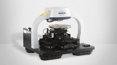
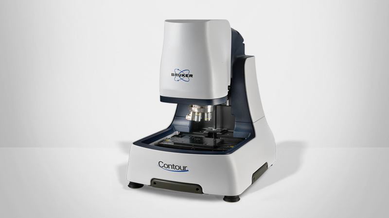
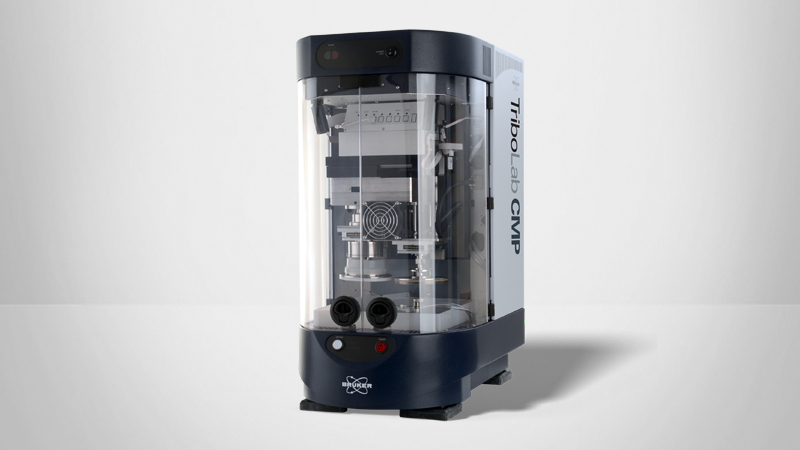
Our automated metrology solutions enable the streamlining of nanomechanical property sampling, from nanoscale-to-microscale indentation to surface roughness measurement, chemical mechanical planarization (CMP), and etch-depth measurements on the most current technology nodes and wafers.
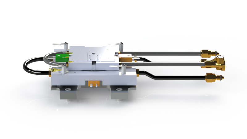
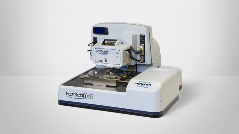
We demonstrate the capabilities of high-resolution, in-situ scanning probe microscopy (SPM) imaging, high-speed mechanical property mapping, and Optical (WLI) Profiling and Stylus Profiling to provide an in-depth explorationof material behavior at the nanoscale, ideal for R&D and the monitoring and improvement of manufacturing processes.
This webinar was presented on April 21, 2021.
Find out more about the technology featured in this webinar or our other solutions for surface characterization of semiconductor materials: