AFM-Based Characterization of the Properties of 2D Materials and Heterostructures
Gain a Deeper Understanding of 2D Materials and their Properties Using AFM
During this webinar, experts discuss how atomic force microscopy (AFM) can be effectively leveraged to understand the structure and properties of 2D materials.
This webinar comprises three presentations:
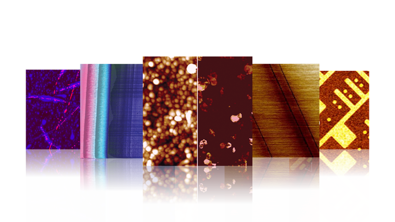
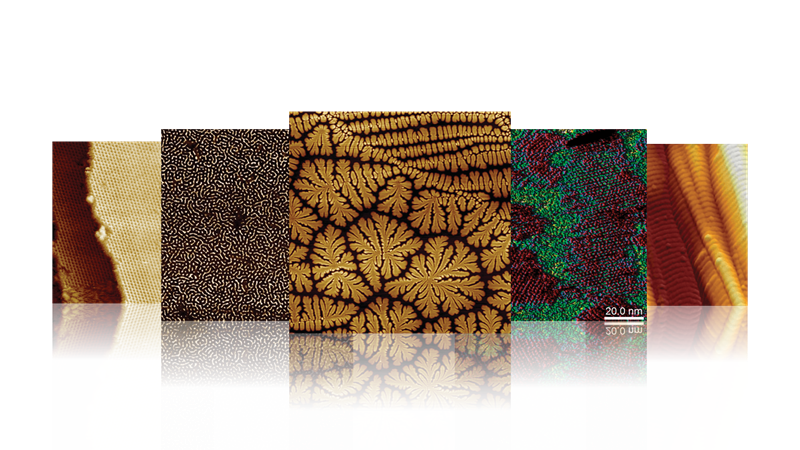
- Bede Pittenger, PhD (Bruker), reviews a broad assortment of AFM-based modes and how they can be used to understand 2D materials and heterostructures.
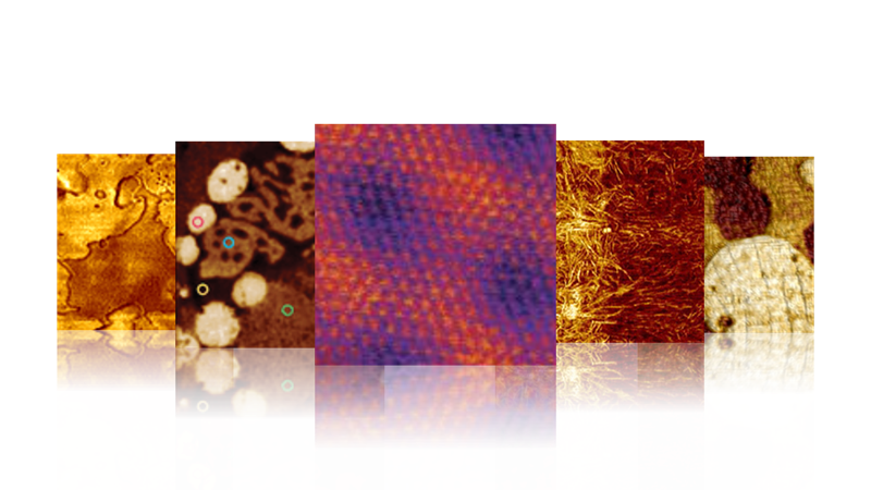
- Mihir Pendharkar, PhD (Stanford University), discusses the development of torsional force microscopy to image moiré superlattices in Van der Waals materials.
- Mario Lanza, PhD (King Abdullah University of Science and Technology), presents about the nanoelectrical properties of the 2D layered material hexagonal boron nitride.
Webinar Summary
Two-dimensional materials have recently been of increasing interest due to observations of their novel optical, mechanical, and electrical properties. Twisted multilayers create moiré superlattices where the properties change with twist angle. Scanning probe microscopy (SPM) methods like atomic force microscopy (AFM) and scanning tunneling microscopy (STM) have proven to be extremely useful in characterizing and understanding these materials due to their high resolution and sensitivity to various different sample properties. In this webinar, we discuss:
- Commonly used SPM modes for identification and characterization of 2D materials
- Recent advancements in consistency of high-resolution 2D material mapping
- Characterization of nanoelectrical properties in 2D materials
- Influence of the fabrication process on 2D material properties
Find out more about the technology featured in this webinar or our other solutions for AFM-Based Characterization:
| Presenter | Presentation Title | Abstract |
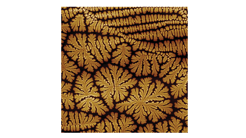
| Bede Pittenger, Ph.D. | Probing 2D materials with the power of AFM | Atomic Force Microscopy was one of the first methods applied to the study of graphene and continues to be a powerful tool for 2D material research in general. Identifying and characterizing single layers and multilayers is routine, while crystal orientation can often be determined with the proper choice of mode and probe. Since the AFM probe can act as a nanoscale electrode, it is possible to directly measure electrical properties of these materials at the relevant length scales between 1 and 100nm. The AFM probe can also be used for nanomanipulation, allowing device fabrication by cutting, folding, or oxidation. In this webinar, we review an assortment of AFM based modes and discuss how they can be used to better understand 2D materials and heterostructures. |
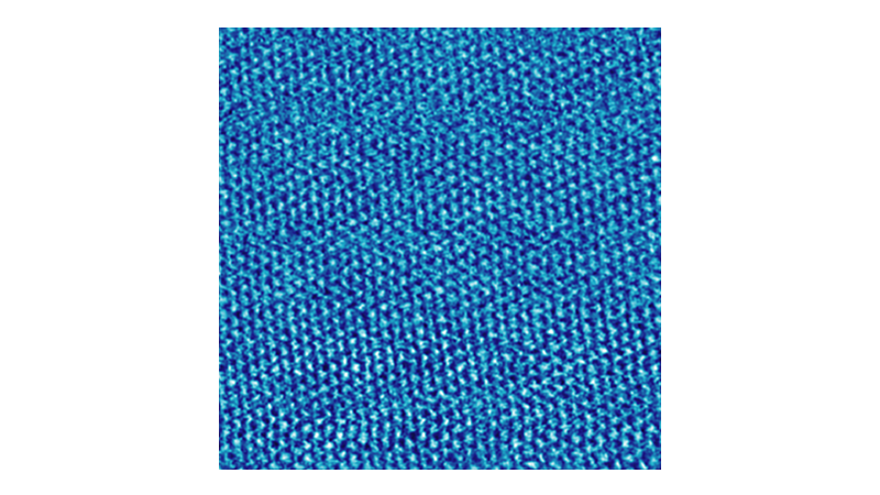
| Mihir Pendharkar, Ph.D. | Torsional Force Microscopy of Van der Waals Moirés and Atomic Lattices | An interlayer twist between two layers of the same Van der Waals (VdW) material (like twisted bilayer graphene (tBG)) creates moiré superlattices with period proportional to the local interlayer twist angle and strain. Moiré patterns are also formed when two atomically thin, dissimilar materials, are placed on top of each other (like graphene on hBN); the moiré period now being sensitive to the difference in the two lattice constants, and their interlayer twist and strain. The moiré period can vary from sub-nanometers to microns in common VdW heterostructures and techniques to directly visualize individual moiré unit cells, over areas as large as common opto-electronic devices (>microns), in air, at room temperature, without extensive sample preparation are scarce. Here, we introduce Torsional Force Microscopy (TFM) - an AFM based technique relying on the torsional resonance of an AFM cantilever - to image moiré superlattices in VdW materials [1]. TFM is sensitive to dynamic friction at the tip-sample interface and hence does not require extensive sample preparation (including nanofabrication) or electrical bias between the tip and the sample. We also find that TFM can reveal atomic lattices of common VdW surfaces like hBN and graphene and can also reveal subsurface moirés, in samples where more than one moiré may exist. TFM was tested to work on VdW heterostructures held on soft polymer stamps and on glass slides, validating its used as a rapid feedback tool in VdW device stacking. With a success rate in excess of 90% for imaging tBG moirés and near certainty of imaging atomic lattices of hBN, TFM should enable unprecedented control over VdW device design, fabrication and feedback. [1] arXiv:2308.08814 |
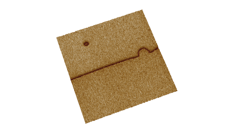
| Mario Lanza, Ph.D. | Nanoelectronic characterization of hexagonal boron nitride using CAFM. | In this webinar I will discuss about the nano-electronic properties of a two-dimensional (2D) layered material called hexagonal boron nitride (h-BN). This material is of special importance for the community because it has a wide band hap of 5.9 eV, and hence it can be used as dielectric in electronic devices, with a perfect van der Waals interface with 2D conductors (like graphene, MXene) and 2D semiconductors (like MoS2, WS2). I will show how the properties of h-BN change depending on the fabrication process followed, focusing specially in samples synthesized by chemical vapour deposition because that is the method preferred by the semiconductors industry. I will mainly show data collected via conductive atomic force microscopy, although I will complement it with that obtained via electron microscopy. |