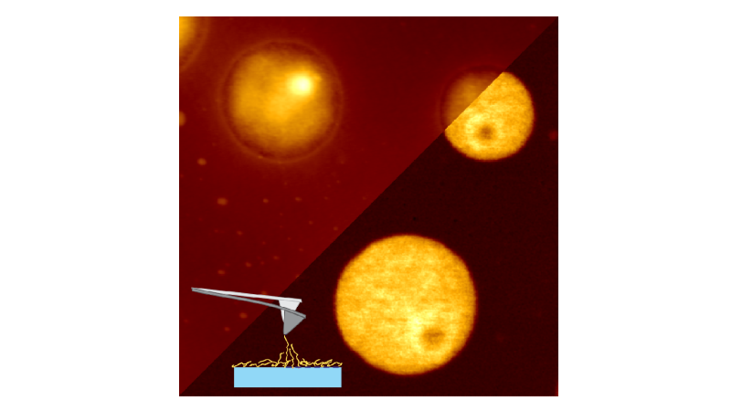
Microscopes

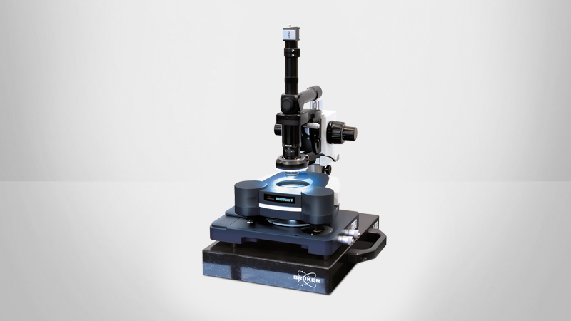
Materials Research AFMs

Helping scientists discover, understand and publish in evolving subjects of materials science

High-Resolution Atomic Force Microscopes for Challenging Research

The atomic force microscope (AFM), now entering its fourth decade as a primary technology for advanced materials research, has been used to drive discovery across a nearly countless array of disciplines and applications.


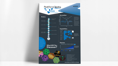
Bruker has led the expansion of atomic force microscope capabilities, starting with the introduction of the first commercial system in the 1980s. Since then, our commitment to helping you do more, and do it more easily, has kept Bruker AFMs at the very cutting-edge of instrumentation innovation. As the technology has matured, our AFMs — powered by exclusive PeakForce Tapping® technology — have consistently delivered highly reliable high-resolution data and empowered scientists to characterize features on ever more complex samples. This data quality and reliability extends to more than just topography; scientists in leading labs around the world are using Bruker AFMs to advance new nanomechanical, nanoelectrical, and nanoelectrochemical research, on the order of three peer-reviewed published articles per day.

Products

Find the Best Atomic Force Microscope for Your Application

Need help? Contact us to discuss your requirements or see our recommendations for instrument selection.

See how to use upgrades and add-ons to customize a Dimension Icon AFM with extended capabilities.

What is an AFM probe?

What is an AFM probe?

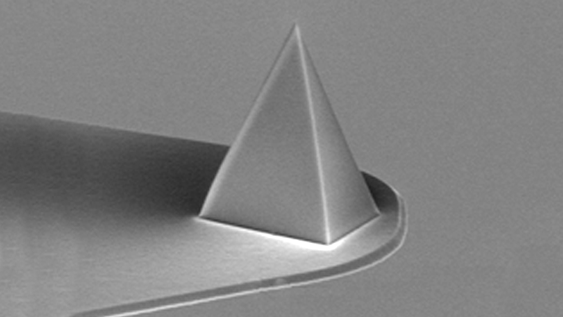
An atomic force microscope uses a probe to measure tip-sample forces as the tip presses against the sample. The AFM probe is a consumable that consists of a sharp tip on a free-moving cantilever mounted on a chip. One or several cantilevers can be mounted on a comparatively large silicon chip (Figure 1).

The geometry and material of both cantilever and tip can be optimized for a given application, resulting in a large library of probe options.


Figure 1. A single silicon chip containing multiple probes.


What are atomic force microscope probes made of?

What are AFM probes made of?

Most AFM probes are made from silicon or silicon nitride. Silicon probes enable stiffer cantilevers and sharper tips, while silicon nitride probes are more durable and flexible. Bruker’s TappingMode probes are generally made from silicon, and contact mode and ScanAsyst probes are generally made from silicon nitride. There is a considerable amount of functionality and flexibility when modifying these common AFM probe materials with coatings or replacing them with individual molecules of interest. The geometry and material of both cantilever and tip can be optimized for a given application, resulting in a large library of probe options on www.BrukerAFMprobes.com.

How do you choose the best AFM probe for your application and sample?

How do you choose the best AFM probe for your application and sample?

The elements of a “good” AFM probe are application-dependent. As such, choosing the right AFM probe relies on balancing parameters of interest including stiffness, spring constant, resonant frequency, and quality factor while considering the needs of your application and the AFM mode used.

Watch our 2023 webinar "The Fundamentals of AFM Probe Selection" to learn about the functional and experimental considerations for selecting a probe, or our 2024 AFM Probes Webinar to hear our AFM experts' recommendations for probe selection.

Where can you buy atomic force microscope probes?

Where can you buy AFM probes?

Bruker is the only major AFM equipment manufacturer that also owns and operates a probes nanofabrication facility, and our broad experience enables us to design and fabricate a wide range of probe types to directly address the evolving needs of AFM users. For more information and to place an order, visit www.BrukerAFMprobes.com.

AFM Modes

Expand Your Research with World's Best Selection of AFM Modes

With an unrivalled — and still growing — suite of available imaging modes, Bruker has an AFM technique for every investigation.

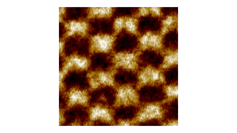
Bruker AFM modes allow researchers to probe their samples’ electrical, magnetic, or materials properties at the nanoscale with unmatched confidence. Bruker’s proprietary PeakForce Tapping technology represents a new core imaging paradigm that provides unprescedented high-resolution imaging, extends AFM measurements into a range of samples not previously accessed, and uniquely enables simultaneous nanoscale property mapping.

This and our other AFM mode advances — such as DataCube, Ringing, ss-PFM, and our new Torsional Resonance Dynamic Friction Microscopy (TR-DFM) modes — are enhancing other correlative and quantitative mapping techniques to enable the development of new modes and deliver new possibilities in an ever-expanding set of topograhical, mechanical, electrical, and chemical applications.

AFM FAQs

Frequently Asked Questions

What is an atomic force microscope?

What is an atomic force microscope?

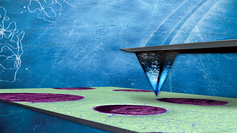
An atomic force microscopy (AFM) is a type of scanning probe microscope (SPM). It uses a very sharp probe that is raster-scanned to produce a true 3D topographical map of the surface of a sample with nanoscale resolution.

How does an atomic force microscope work?

How does an atomic force microscope work?

All types of scanning probe microscopes use a physical probe touching the surface of a sample to scan the surface and collect data. However, their measurement mechanisms are very different — an atomic force microscope uniquely measures the cantilever deflection (bending) caused by forces between the tip and the sample surface. As a result, atomic force microscopes can be used to measure a much wider range of materials than STM.

The basic working principle of an atomic force microscope is:

  1. A sharp tip at the free end of a cantilever is raster-scanned over a small area of sample.
  2. As the tip passes over the surface, variations in height cause the cantilever to bend.
  3. This bending, or change in deflection, is detected through movement of a laser or super luminescent diode (SLD) that is reflected off the cantilever into a position-sensitive photodetector (PSPD).

Throughout this process, piezo actuators operate within an electronic feedback loop to move the tip or sample closer or further away from each other to maintain the relative tip-sample distance and a constant setpoint. 


What are the advantages of using an atomic force microscope for materials research?

What are the advantages of using an atomic force microscope for materials research?

The following table compares methods commonly used to characterize materials at the nanoscale and can be used to understand:

  • What is the difference between AFM and SEM?
  • What is the difference between AFM and STM?
  • What is the difference between AFM and TEM? and
  • What is the difference between AFM and confocal microscopy?

Each technique has a great deal of nuance, and values given are approximations. The green marker indicates “definitely yes," the yellow marker indicates “sometimes yes, with additional considerations," and the red marker indicates “definitely no."

  AFM STM SEM TEM Confocal
3D Imaging 🟩 🟩 🟨 🟨 🟩
Measurements in Vacuum 🟩 🟩 🟩 🟩 🟥
Measurements in Air 🟩 🟥 🟥 🟥 🟩
Measurements in Liquid 🟩 🟥 🟥 🟥 🟩
Label-Free Experiments 🟩 🟩 🟩 🟩 🟥
Appx. Lateral Resolution (nm) 1 0.1 1-10 0.05-05 200
Appx. Vertical Resolution (nm) 0.1 0.1 N/A N/A 500
Sample Requirements/Limitations Very few limitations
Limited to conductive samples Limited to conductive or coated samples Limited to sample thickness <100 nm Samples must be tagged
AFM Applications

Investigate Properties in Nanoscale Structures

What are atomic force microscopes used for?

What are atomic force microscopes used for?

Atomic force microscopes are used in a wide variety of research and industry applications to collect information about the nanoscale structure and properties of almost any type of sample.

What kinds of observations can be made with atomic force microscopes?

What kinds of observations can be made using an atomic force microscope?

While atomic force microscopy is best known for its ability to resolve surface structure, it provides valuable information about other material properties at the nanoscale. These include mechanical, electrical, electrochemical, piezoelectric, magnetic, thermal, and optical properties. AFM can also be used to manipulate a sample (push, pull, or write) in nanolithography and intra-/inter-molecular (un)binding studies.

With a large variety of measurement types and high degree of sample flexibility, AFM has become a fundamental nano-characterization technique in both academic research and industry for a range of applications, including:

Resources

Learn More About Atomic Force Microscopy

Bruker has deep experience and expertise in all things related to atomic force microscopy.

We are eager to share this knowledge with the larger research community. Be sure to explore our extensive offering of resources, below.

If you would like to speak with a Bruker atomic force microscopy expert in person, contact us to discuss your specific application requirements and measurement needs.

Watch Our AFM Webinars

Our webinars cover best practices, introduce new products, provide quick solutions to tricky questions, and offer ideas for new applications, modes, or techniques.
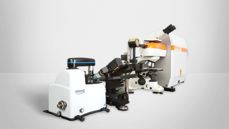
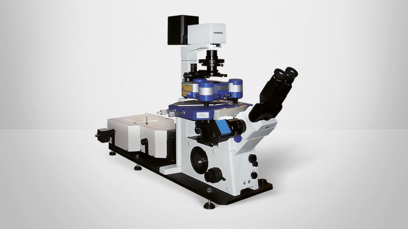
Publications

Browse Atomic Force Microscopy Articles

Article Year Article Title Authors AFM System Mode Research Area
2022 Implementation of an Experimental Setup to Qualitatively Detect Hydrogen Permeation Along Grain Boundaries in Nickel Using Scanning Kelvin Probe Force Microscopy Under Varying Atmospheres Gruenewald, P.; Hautz, N.; Motz, C. Icon PeakForce KPFM Fuel Cell, Nanoelectrical
2019 Nanoscale DMA With the Atomic Force Microscope: A New Method for Measuring Viscoelastic Properties of Nanostructured Polymer Materials Pittenger, B.; Osechinskiy, S.; (…); Mueller, T. Icon AFM-nDMA Polymers, Nanomechanical
2021 Investigating the Relationship Between the Mechanical Properties of Plasma Polymer-Like Thin Films and Their Glass Transition Temperature Vinx, N.; Damnan, P.; (…); Thiry, D. Icon AFM-nDMA, PeakForce QNM Polymers, Nanomechanical
2020 Comparison of Fresh and Aged Lithium Iron Phosphate Cathodes Using a Tailored Electrochemical Strain Microscopy Technique Simolka, M.; Kaess, H.; Friedrich, K. A. Icon AFM-nDMA, PeakForce QNM Batteries, Nanomechanical, Nanoelectrochemical
2020 Nanoscale Viscoelastic Characterization of Asphalt Binders Using the AFM-nDMA Test Aljarrah, M.; Masad, E. Icon AFM-nDMA, PeakForce QNM Bitumen, Nanomechanical
2021 Analysis of LiCoO₂ Electrodes Through Principal Component Analysis of Current–Voltage Datacubes Measured Using Atomic Force Microscopy Maeda, Y.; Taguchi, N.; Sakaebe, H. Icon Datacube, Scanning Spreading Resistance Microscopy (SSRM) Batteries, Nanoelectrical
2017 Morphology Dynamics of Single-Layered Ni(OH)2/iOOH Nanosheets and Subsequent Fe Incorporation Studied by in Situ Electrochemical Atomic Force Microscopy Deng, J.; Nellist, M. R.; (…); Boettcher, S. W. Icon Electrochemical AFM (EC-AFM) Batteries, Nanoelectrochemical
2020 Failure Progression in the Solid Electrolyte Interphase (SEI) on Silicon Electrodes Guo, K.; Kumar, R.; (…); Gao, H. Icon Electrochemical AFM (EC-AFM); PeakForce Tapping Batteries, Nanoelectrochemical
2018 Structural Evolution of Metal (Oxy)hydroxide Nanosheets During the Oxygen Evolution Reaction Dette, C.; Hurst, M. R.; (…); Boettcher, S. W. Icon Electrochemical AFM (EC-AFM); PeakForce Tapping Fuel Cells, Nanoelectrochemical
2021 Signal Origin of Electrochemical Strain Microscopy and Link to Local Chemical Distribution in Solid State Electrolytes Schön, N.; Schierholz, R.; (…); Hausen, F. Icon Electrochemical Strain Microscopy (ESM) Batteries, Nanoelectrochemical
2018 Imaging Photogenerated Charge Carriers on Surfaces and Interfaces of Photocatalysts With Surface Photovoltage Microscopy Chen, R.; Fan, F.; (…); Li, C. Icon Kelvin Force Probe Microscopy (KPFM) Fuel Cells, Nanoelectrical
2017 Visualizing the Nano Cocatalyst Aligned Electric Fields on Single Photocatalyst Particles Zhu, J.; Pang, S.; (…); Li, C. Icon Kelvin Force Probe Microscopy (KPFM) Fuel Cells, Nanoelectrical
2018 A Facile Space-Confined Solid-Phase Sulfurization Strategy for Growth of High-Quality Ultrathin Molybdenum Disulfide Single Crystals Li, D.; Xiao, Z.; (…); Lu, Y. MultiMode Kelvin Probe Force Microscopy (KPFM); Piezoresponse Force Microscopy (PFM) 2D Materials, Nanoelectrical
2018 Twistable Electronics With Dynamically Rotatable Heterostructures Ribeiro-Palau, R.; Zhang, C.; (…); Dean, C. R. Icon Lateral Force Microscopy (LFM) 2D Materials, Nanomechanical
2021 Large-Area, Two-Dimensional MoS2 Exfoliated on Gold: Direct Experimental Access to the Metal–Semiconductor Interface Pollmann, E.; Sleziona, S.; (…); Schleberger, M. Icon PeakForce KPFM 2D Materials, Nanoelectrical
2021 Band Edge Energy Tuning through Electronic Character Hybridization in Ternary Metal Vanadates Richter, M. H.; Peterson, E. A.; (…); Gregoire, J. M. Icon PeakForce KPFM Nanoelectrical
2020 Intergranular Corrosion Behavior of Low-Chromium Ferritic Stainless Steel Without Cr-Carbide Precipitation After Aging Hu, S.; Mao, Y.; (…); Hänninen, H. Icon PeakForce KPFM Metals, Nanoelectrical
2021 Long-Term Corrosion Behavior of the 7A85 Aluminum Alloy in an Industrial-Marine Atmospheric Environment Zhao, Q.; Guo, C.; (…); Li, X. MultiMode PeakForce KPFM Metals, Nanoelectrical
2021 Microstructure – Electron Work Function Relationship: A Crucial Step Towards “Electronic Metallurgy” Luo, Y.; Tang, Y.; (…); Li, D.Y. MultiMode PeakForce KPFM Metals, Nanoelectrical
2021 Electron Work Function: An Indicative Parameter Towards a Novel Material Design Methodology Luo, Y.; Tang, Y.; (…); Li, D. Y. MultiMode PeakForce KPFM Nanoelectrical
2021 Fusion of Purple Membranes Triggered by Immobilization on Carbon Nanomembranes Riedel, R.; Frese, N.; (…); Gölzhäuser, A. MultiMode PeakForce KPFM Nanoelectrical
2021 In situ Investigation of Oxidation Across a Heterogeneous Nanoparticle–Support Interface During Metal Support Interactions Datta, A.; Deolka, S.; (…); Porkovich, A. J. MultiMode PeakForce KPFM Nanoparticles, Nanoelectrical
2021 Defect-Assisted Electronic Metal–Support Interactions: Tuning the Interplay Between Ru Nanoparticles and CuO Supports for pH-Neutral Oxygen Evolution Porkovich, A. J.; Kumar, P.; (…); Datta, A. MultiMode PeakForce KPFM Nanoparticles, Nanoelectrical
2020 Understanding Crystallographic Orientation Dependent Dissolution Rates of 90Cu-10Ni Alloy: New Insights Based on AFM/SKPFM Measurements and Coordination Number/Electronic Structure Calculations Ma, A.; Zhang, L.; (…); Zheng, Y. MultiMode PeakForce KPFM Metals, Nanoelectrical
2017 Electron Work Function – A Probe for Interfacial Diagnosis Li, D. Y.; Guo, L.; (…); Lu, H. MultiMode PeakForce KPFM Nanoelectrical, Corrosion
2022 Surface Properties and Architectures of Male Moth Trichoid Sensilla Investigated Using Atomic Force Microscopy Baker, T. C.; Zhou, Q.; (…); Tighe, T. B. Icon PeakForce KPFM, PeakForce QNM Biology, Nanoelectrical, Nanomechanical
2021 Structurally Driven Environmental Degradation of Friction in MoS2 Films Curry, J. F.; Ohta, T.; (…); Chandross, M. Icon PeakForce KPFM, PeakForce QNM 2D Materials, Nanoelectrical, Nanomechanical
2020 A Mesoporous Catalytic Fiber Architecture Decorated by Exsolved Nanoparticles for Reversible Solid Oxide Cells Zhou, J.; Yang, J.; (….); Wu, K. Icon PeakForce KPFM, PeakForce QNM Metals, Nanoelectrical, Nanomechanical
2020 The Optical Signatures of Molecular-Doping Induced Polarons in Poly(3-hexylthiophene-2,5-diyl): Individual Polymer Chains Versus Aggregates Mansour, A. E.; Lungwitz, D.; Schultz, (…); Koch, N. Icon PeakForce KPFM, PeakForce QNM Nanoelectrical
2020 Highly Selective Carrier-Type Modulation of Tungsten Selenide Transistors Using Iodine Vapor Fan, S.; Cao, M.; (…); Su, J. Icon PeakForce KPFM, PeakForce QNM Nanoelectrical
2020 Oxidation Promoted Self-Assembly of π-Conjugated Polymers Hicks, G. E. J.; Jarrett-Wilkins, C. N.; (…); Seferos, D. S. Icon PeakForce KPFM, PeakForce QNM Polymers, Nanoelectrical
2021 Extremely Fast Optical and Nonvolatile Control of Mixed‐phase Multiferroic BiFeO3 via Instantaneous Strain Perturbation Liou, Y-D.; Ho, S-Z.; (…); Yang, J-C. Icon PeakForce KPFM, Piezoresponse Force Microscopy (PFM) Ferroelectrics, Nanoelectrical
2020 Assessment of AFM - KPFM and Scanning Spreading Resistance Microscopy (SSRM) for Measuring and Characterizing Materials Aging Processes Baca, Ana Icon PeakForce KPFM, Piezoresponse Force Microscopy (PFM) Nanoelectrical
2021 Mechanical Properties of Organic Electronic Polymers on the Nanoscale Panchal, V.; Dobryden, I.; (…); Venkateshvaran, D. FastScan PeakForce QNM Polymers, Nanomechanical
2019 Automated Multi-Sample Acquisition and Analysis Using Atomic Force Microscopy for Biomedical Applications Dujardin, A.; De Wolf, P.; (…); Dupres, V. FastScan PeakForce QNM Biology, Automation
2019 Lithium Anode Stable in Air for Low-Cost Fabrication of a Dendrite-Free Lithium Battery Shen, X.; Li, Y.; (…); Goodenough, J. B. Icon PeakForce QNM Batteries, Nanomechanical
2021 Nano-Vault Architecture Mitigates Stress in Silicon-Based Anodes for Lithium-Ion Batteries Haro, M.; Kumar, P.,(…); Grammatikopoulos, P. MultiMode PeakForce QNM Batteries, Nanomechanical
2020 Layer-by-Layer Printing of Photopolymers in 3D: How Weak is the Interface? Gojzewski, H.; Guo, Z.; (…); Vancso, G. J. MultiMode PeakForce QNM Additive Manufacturing, Nanomechanical
2021 Nanoscale Redox Mapping at the MoS2-Liquid Interface Du, H.; Huang,Y.; (…); Chen, L. Icon PeakForce SECM 2D Materials, Nanoelectrical, Nanoelectrochemical
2019 Nanoscale Semiconductor/Catalyst Interfaces in Photoelectrochemistry Laskowski, F. A. L.; Oener, S. Z.; (…); Boettcher, S. W. Icon PeakForce SECM Fuel Cells, Nanoelectrochemical
2018 Potential-Sensing Electrochemical Afm Shows CoPi as a Hole Collector and Oxygen Evolution Catalyst on BiVO4 Water-Splitting Photoanodes Nellist, M. R.; Qiu, J.; (…); Boettcher, S. W. Icon PeakForce SECM Fuel Cells, Nanoelectrochemical
2017 Potential-Sensing Electrochemical Atomic Force Microscopy for in Operando Analysis of Water-Splitting Catalysts and Interfaces Nellist, M. R.; Laskowski, F. A. L.; (…); Boettcher, S. W. Icon PeakForce SECM Fuel Cells, Nanoelectrochemical
2017 Atomic Force Microscopy With Nanoelectrode Tips for High Resolution Electrochemical, Nanoadhesion and Nanoelectrical Imaging Nellist, M. R.; Chen, Y.; (…); Boettcher, S. W. Icon PeakForce SECM Nanoelectrochemical
2017 Nanoelectrical and Nanoelectrochemical Imaging of Pt/p-Si and Pt/p+-Si Electrodes Jiang, J.; Huang, Z.; (…); Brunschwig, B. S. Icon PeakForce SECM, PeakForce TUNA Fuel Cells, Nanoelectrical, Nanoelectrochemical
2020 Capillary Condensation Under Atomic-Scale Confinement Yang, Q.; Sun, P.; (…); Geim, A. FastScan, Icon PeakForce Tapping 2D Materials
2020 Supramolecular Copolymerization Driven by Integrative Self‑Sorting of Hydrogen-Bonded Rosettes Aratsu, K.; Takeya, R.; (…); Yagai. S. MultiMode PeakForce Tapping Polymers, Molecules
2021 Optimized Atomic Layer Deposition of Homogeneous, Conductive Al2O3 Coatings for High-Nickel NCM Containing Ready-to-Use Electrodes Negi, R. S.; Culver, S. P.; (…); Elm, M. T. Icon PeakForce TUNA Batteries, Nanoelectrical
2021 On the Importance of Li Metal Morphology on the Cycling of Lithium Metal Polymer Cells Storelli, A.; Rousselot, S.; (…); Dollé, M. Icon PeakForce TUNA Batteries, Nanoelectrical
2021 Conducting Composite Films Based on Chitosan or Sodium Hyaluronate. Properties and Cytocompatibility With Human Induced Pluripotent Stem Cells Jasenská, D.; Kašpárková, V.; (…); Humpolíček, P. Icon PeakForce TUNA Biology, Nanoelectrical
2021 Development of a Photoelectrochemically Self-Improving Si/GaN Photocathode for Efficient and Durable H2 Production Zeng, G.; Pham, T. A.; (…); Toma, F. M. Icon PeakForce TUNA Fuel Cells, Nanoelectrical
2021 Fabrication of PCDTBT Conductive Network via Phase Separation Xu, J.; Liu, Z.; (…); Chen, J. Icon PeakForce TUNA Nanoelectrical
2021 Spatiotemporal Imaging of Anisotropic Charge Transfer in Photocatalyst Particles Li, C.; Chen, R.; (…); Fan, F. Icon PeakForce TUNA Nanoparticles, Nanoelectrical
2021 Current Rectification and Photo-Responsive Current Achieved through Interfacial Facet Control of Cu2O–Si Wafer Heterojunctions Lee, A-T.; Tan, C-S.; Huang, M. H. Icon PeakForce TUNA Photovoltaics, Nanoelectrical
2021 Correlation of Thermoelectric Performance, Domain Morphology and Doping Level in PEDOT:PSS Thin Films Post‐Treated With Ionic Liquids Oechsle, A. L.; Heger, J. E.; (…); Müller‐Buschbaum, P. Icon PeakForce TUNA Photovoltaics, Polymers, Nanoelectrical
2021 Electrically Conductive Silicon Oxycarbide Thin Films Prepared From Preceramic Polymers Ricohermoso, E. III, Klug, F.; (…); Ionescu, E. Icon PeakForce TUNA Polymers, Nanoelectrical
2021 Gate‐Controlled Polarity‐Reversible Photodiodes With Ambipolar 2D Semiconductors Du, J.; Liao, Q.; (…); Zhang, Y. Icon PeakForce TUNA Semiconductors, Nanoelectrical
2021 Influence of Surface Band Bending on a Narrow Band Gap Semiconductor: Tunneling Atomic Force Studies of Graphite With Bernal and Rhombohedral Stacking Orders Ariskina, R.; Schnedler, M.; (…); Estrela-Lopis, I. Icon PeakForce TUNA Semiconductors, Nanoelectrical
2020 Surface Defects State Analysis of Laser Induced Graphene From 4H-SiC Lin, Z.; Ji, L.; (…); Sun, Z. Icon PeakForce TUNA 2D Materials, Nanoelectrical
2020 Effects of the Mixing Sequence on Making Lithium Ion Battery Electrodes Wang, M.; Dang, D.; (…); Cheng, Y-T. Icon PeakForce TUNA Batteries, Nanoelectrical
2020 Harnessing Silicon Facet-Dependent Conductivity to Enhance the Direct-Current Produced by a Sliding Schottky Diode Triboelectric Nanogenerator Ferrie, S.; Darwish, N.; (…); Ciampi, S. Icon PeakForce TUNA Nanoelectrical
2020 Time-Resolved Open-Circuit Conductive Atomic Force Microscopy for Direct Electromechanical Characterization Calahorra, Y.; Kim, W.; (…); Kar-Narayan, S. Icon PeakForce TUNA Nanoelectrical
2020 Local Defect-Enhanced Anodic Oxidation of Reformed GaN Nanowires Colvin, J.; Ciechonski, R.; (…); Timm, R. Icon PeakForce TUNA Nanowires, Nanoelectrical
2020 Silver Nanofilament Formation Dynamics in a Polymer‐Ionic Liquid Thin Film by Direct Write Chao, Z.; Sezginel, K. B.; (…); Fullerton‐Shirey, S. K. Icon PeakForce TUNA Polymers, Nanoelectrical
2020 Nanoscale Observation of the Solid Electrolyte Interface and Lithium Dendrite Nucleation–Growth Process During the Initial Lithium Electrodeposition Wang, S.; Yin, X.; (…); Li, B. Icon PeakForce TUNA
2019 In Situ Observation of the Insulator-to-Metal Transition and Nonequilibrium Phase Transition for Li1–xCoO2 Films With Preferred (003) Orientation Nanorods Chen, Y.; Yu, Q.; (…); Huang, Z. Icon PeakForce TUNA Batteries, Nanowires, Nanoelectrical
2019 Relation Between Charge Transport and the Number of Interconnected Lamellar Poly(3-Hexylthiophene) Crystals Wang, B.; Chen, J.; (…); Zhang, B. Icon PeakForce TUNA Polymers, Nanoelectrical
2018 Electrically Controlled Water Permeation Through Graphene Oxide Membranes Zhou, K-G.; Vasu, K. S.; (…); Nair, R. R. Icon PeakForce TUNA 2D Materials, Nanoelectrical
2018 Nanoscale Imaging of Charge Carrier Transport in Water Splitting Photoanodes Eichhorn, J.; Kastl, C.; (…); Toma, F. M. Icon PeakForce TUNA Fuel Cells, Nanoelectrical
2017 A Liquid Metal Reaction Environment for the Room-Temperature Synthesis of Atomically Thin Metal Oxides Zavabeti, A.; Ou, J.; (…); Daeneke, T. Icon PeakForce TUNA 2D Materials, Nanoelectrical
2021 Uncapped Gold Nanoparticles for the Metallization of Organic Monolayers Martín‐Barreiro, A.; Soto, R.; (…); Cea, P. Icon, MultiMode PeakForce TUNA Nanoelectrical
2021 Exploring the Interface of Skin‐Layered Titanium Fibers for Electrochemical Water Splitting Liu, C.; Shviro, M.; (…); Carmo, M. MultiMode PeakForce TUNA Fuel Cells, Nanoelectrical
2021 Microscopic Characterization of Poly(Sulfur Nitride) Amado, E.; Hasan, N.; (…); Kressler, J. MultiMode PeakForce TUNA Nanoelectrical
2021 Al2O3 Buffer-Facilitated Epitaxial Growth of High-Quality ZnO/ZnS Core/Shell Nanorod Arrays Ru, F.; Xia, J.; (…); Meng, X-M. MultiMode PeakForce TUNA Nanoelectrical
2020 An Ordered and Fail‐Safe Electrical Network in Cable Bacteria Eachambadi, R. T.; Bonné, R.; (…); Manca, J. V. MultiMode PeakForce TUNA Bacteria, Biology, Nanoelectrical
2020 Stabilizing Polymer–Lithium Interface in a Rechargeable Solid Battery Yan, M.; Liang, J-Y.,(…); Wan, L-J MultiMode PeakForce TUNA Batteries, Nanoelectrical
2020 Ultrafast Assembly of Swordlike Cu3(1,3,5-Benzenetricarboxylate)n Metal–Organic Framework Crystals With Exposed Active Metal Sites Ahmed, H.; Yang, X.; (…); Yeo, L. Y. MultiMode PeakForce TUNA Metals, Nanoelectrical
2020 Sn/SnO Hybrid Graphene for Thermal Interface Material and Interconnections With Sn Hybrid Carbon Nanotubes Mittal, J.; Lin, K. L. PeakForce TUNA Nanoelectrical
2021 Non-Destructive Depth-Dependent Morphological Characterization of Ferroelectric:Semiconducting Polymer Blend Films Spampinato, N.; Pecastaings, G.; (…); Pavlopoulou, E. Icon PeakForce TUNA Polymers, Nanoelectrical
2018 Determination of Polypeptide Conformation With Nanoscale Resolution in Water Ramer, G.; Ruggeri, F. S.; (…); Centrone, A. NanoIR Photothermal AFM-IR Biology, Molecules, Nanochemical
2019 Deterministic Optical Control of Room Temperature Multiferroicity in BiFeO3 Thin Films Liou, Y-D.; Chiu, Y-Y.; (…); Yang, J-C. MultiMode Piezoresponse Force Microscopy (PFM) Ferroelectrics, Nanoelectrical
2018 Poling-Free Energy Harvesters Based on Robust Self-Poled Ferroelectric Fibers Zhu, R.; Wang, Z.; (…); Kimur, H. MultiMode Piezoresponse Force Microscopy (PFM) Ferroelectrics, Nanoelectrical
2017 Temporary Formation of Highly Conducting Domain Walls for Non-Destructive Read-Out of Ferroelectric Domain-Wall Resistance Switching Memories Jiang, J.; Bai, Z. L.; (…); Jiang A. Q. Icon Piezoresponse Force Microscopy (PFM); Kelvin Probe Force Microscopy (KPFM) Ferroelectrics, Nanoelectrical
2018 Unidirectional Molecular Assembly Alignment on Graphene Enabled by Nanomechanical Symmetry Breaking Hong, L.; Nishihara, T.; (…); Itami, K. FastScan TappingMode 2D Materials, Molecules
2020 Controlling MOFS ZnO Heterostructure Kinetics Through Selective Ligand Binding to ZnO Surface Steps Tao, J.; Lee, M-S.; (…); Sinnwell, M. A. MultiMode TappingMode
2021 Reversible Planar Gliding and Microcracking in a Single‑Crystalline Ni-Rich Cathode Bi, Y.; Tao, J.,(…); Xiao, J. MultiMode Batteries, Nanoelectrochemical
Service and Support

How Can We Help?

Bruker partners with our customers to solve real-world application issues. We develop next-generation technologies and help customers select the right system and accessories. This partnership continues through training and extended service, long after the tools are sold.

Our highly trained team of support engineers, application scientists and subject-matter experts are wholly dedicated to maximizing your productivity with system service and upgrades, as well as application support and training.

Contact Us

Input value is invalid.

* Please fill out the mandatory fields.

Please enter your first name
Please enter your last name
Please enter your e-mail address
Please enter a valid phone number
Please enter your Company/Institution
What best describes your current interest?
I would like to receive related product announcements, webinar invitations, and event information via email. [NOTE: You can opt-out at any time].
Please accept the Terms and Conditions