Application Note: Accelerated Correlation of Microstructure–Mechanical Property Relationships in Laser Clad Steel
Efficient Correlation of Local Structure and Properties
Understanding structure‑property relationships is a core tenet of materials science, and direct correlation of microstructure with resulting local mechanical properties is highly valued in many applications. Conventional co‑located data collection for a correlation analysis follows the process of measure → transfer → locate → measure, transferring between a microscope and a nanoindenter. This workflow is inefficient and prone to introducing errors due to misalignment or sample damage during transfer. The PI 89 Auto SEM PicoIndenter overcomes these limitations by enabling direct, targeted nanoindentation in the scanning electron microscope (SEM) via a dual‑axis rotation and tilt (R/T) stage. Within a single platform, users can select features in electron or EDS/EBSD images and immediately indent at those same coordinates, resulting in a straightforward measure → measure workflow.
This application note presents a case study on laser clad steel using PI 89 Auto for co‑located imaging and nanomechanical data collection, resulting in effective and accelerated microstructure–mechanical property correlation.
Readers can expect to find:
- An overview of the PI 89 Auto instrument configuration
- Workflow details for coordinated nanoindentation and SE/BSE/EDS/EBSD imaging
- A case study on laser-clad 410/4140 steel, where PI 89 Auto revealed phase‑dependent hardness variations and mechanical gradients across interfaces
KEYWORDS: Nanomechanical Testing; In-Situ Nanoindentation; Hysitron; AN1551; Bruker; Application Note; SEM PicoIndenter; PI 89 Auto

Instrument Configuration and Workflow Overview
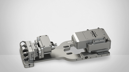
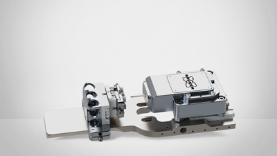
The Hysitron® PI 89 Auto SEM PicoIndenter is an in‑situ nanoindenter designed for seamless integration with SEM workflows. PI 89 Auto features a patented two‑axis R/T stage that adds two degrees of freedom to the base PI 89 platform. The added degrees of freedom enable PI 89 Auto’s stage to be precisely angled for nanoindentation, EBSD, and top‑down SEM imaging — including secondary electron (SE), backscattered electron (BSE), and energy‑dispersive X‑ray spectroscopy (EDS) imaging — without removing the specimen from the chamber (Figure 1).

Instrument control is managed via TriboScan™ software, which communicates directly with Bruker ESPRIT™ EBSD systems. Users can select indent locations based on any imaging modality and move seamlessly to indentation at the targeted position. Calibration is performed once per session to register the indentation and imaging coordinate systems for both SEM‑column and EBSD orientations. This two‑orientation approach ensures reliable targeting for all workflows.
After calibration, users simply select areas of interest from SE/BSE/EDS/EBSD images. Coordinates are then transferred to TriboScan, which calculates and executes at the corresponding indentation position. Targeting is thus reduced to a single click from the imaging modality interface.
Materials and Methods
A 4140 steel substrate was laser clad with 410 stainless steel powder as described in previously published work.1 A cross section of the cladded material was prepared to EBSD quality: ground with SiC metallographic paper to 1200 grit, polished with diamond suspensions, and finished with 10 min of final polishing using 50 nm colloidal alumina.
The PI 89 Auto system in this study was equipped with a 30 μm range piezoelectric actuator, a 500 mN xR high‑load transducer, and a diamond Berkovich probe. Indentation grids were performed with Bruker’s XPM™ accelerated property mapping, operated with displacement control to a maximum depth of 150 nm and 0.1 s segment times for both loading and unloading. One XPM map per region (410, heat affected zone (HAZ), 4140) comprised 25×25 indents over 75×75 μm², with indent spacing of 3 μm to minimize interaction between adjacent indents.2 Each area was scanned with EBSD before indentation, then XPM map coordinates were identified in the EBSD view, and the same area was re‑scanned after indentation to align indents with microstructural features.
To ensure that gradients across interfaces were also captured, a continuous line scan was collected from the 4140 region through into the 410 cladding. The line scan was an XPM load function executed as a line of 825 indents over 2475 μm (3 μm/indent). It began >1 mm from the HAZ (as identified by BSE imaging) to capture bulk 4140 behavior before entering the transition region.
LEARN MORE:
Results and Discussion
Microstructure Analysis
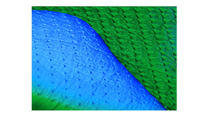
Cross‑section images based on chemistry (EDS) and microstructure (concentric backscatter, CBS) are given in Figure 2 and show three distinct zones. The 410 cladding on the left is rich in Cr, the base 4140 region to the right exhibits distinct grain structure, and the HAZ between them has lower Cr concentration combined with a lack of distinct microstructural features. The HAZ spans 650–800 μm, measured from the Cr interface to the start of the base 4140 grain structure.


Targeted Hardness Mapping
The 410 cladding pre‑indentation EBSD scan (Figure 3a) revealed a two‑phase region with large grains and clusters of precipitates, both of which indexed as ferrite. It is likely that the large grains are ferrite, whereas the precipitates are clusters of tempered martensite.
Indents are visible in the post‑indentation EBSD scan (Figure 3b) due to the high local deformation caused by indentation. The grid itself appears skewed in Figure 3b because of the imaging angle imposed by the pre‑tilt adapter, which is accounted for in targeting calculations. Targeting was precise, with only 16 μm from the targeted position to the edge of the indentation area.
Figure 4a shows the microstructure from Figure 3b rotated to align with the PI 89 axes, for direct comparison with the mechanical maps. The hardness map (Figure 4b) exhibits lower hardness (blue, average 3.01 GPa) in the large ferritic grains and higher hardness (red, average 4.89 GPa) in the martensitic clusters. The reduced modulus map (Figure 4c) mirrors this contrast, with higher modulus in the harder regions.
It should be noted that the high speed of the indentation process may lead to an increased observed material hardness with respect to quasistatic indentation, due to possible material strain rate sensitivity.2 However, all materials were investigated with the same loading profile, enabling valid relative comparisons.


Hardness Profiling Across Clad Interface
Results from the line of indents is given in Figure 5, which has the same orientation as Figure 2 (4140 region on the right and the 410 cladding on the left). Hardness from the line scan remains near 3 GPa across the initial ~1 mm within the 4140 region. Approaching the HAZ, scatter increases and mean hardness rises, peaking around 6 GPa near the Cr interface. Entering the 410 cladding, average hardness decreases, but the scatter becomes bimodal, consistent with the dual‑phase ferritic–martensitic microstructure.
Box‑and‑whisker plots from EBSD‑targeted XPM maps were overlaid on the same distance axis in Figure 5. The hardness distribution from the 4140 grid of indents accurately captures the line‑scan segment data. In the HAZ, a majority of the line‑scan data points lie outside the middle 50% (interquartile range) of the HAZ’s box‑and‑whisker, indicating fair disagreement between the two datasets and reflecting the HAZ’s heterogeneity. The distribution from the XPM data in the 410 cladding aligns with the left‑most cluster of points within the 410 line‑scan segment. Without EBSD, the increased scatter would be ambiguous, but EBSD identifies the higher‑hardness mode as tempered martensite and the lower‑hardness mode as ferrite.
PI 89 Auto Enables Efficient Structure‑Property Correlation
PI 89 Auto enables direct, microstructure‑targeted nanoindentation in the SEM by combining a patented R/T stage with coordinate‑aware software tied to EBSD/EDS. In this study on laser‑clad 410/4140 steel, PI 89 Auto was used to reveal phase‑dependent hardness variations and mechanical gradients across interfaces. Data was collected in a single workday and comprised three EBSD‑targeted XPM maps and one line scan. Each XPM grid required ~2 h (dominated by EBSD scan time), and the line scan required ~1.5 h. This automated correlative workflow presents a notable improvement over traditional multi‑instrument sequences.
Authors
- Kevin Schmalbach, Ph.D., Staff Scientist (kevin.schmalbach@bruker.com)
- Eric Hintsala, Ph.D., Manager NI Applications Development (eric.hintsala@bruker.com)
- Sanjit Bhowmick, Ph.D., NI Product Line Manager (sanjit.bhowmick@bruker.com)
- Douglas Stauffer, Ph.D., Director NI Business Unit (douglas.stauffer@bruker.com)
Acknowledgement
A version of this work was first published by K. Schmalbach et al. in JOM 77, p. 4081–4089, (2025), DOI: 10.1007/s11837-025-07322-1, by Springer Nature.
References
- Haake, J.M., and Zediker, M.S. 2005. “Heat Treating and Cladding Operations with High‑Power Diode Lasers.” Proc. SPIE 5706, Critical Review: Industrial Lasers and Applications, 76–86. DOI: 10.1117/12.601647
- Hintsala, E.D., Hangen, U., and Stauffer, D.D. 2018. “High‑Throughput Nanoindentation for Statistical and Spatial Property Determination.” JOM 70 (4): 494–503. DOI: 10.1007/s11837‑018‑2752‑0