Defects & Contamination

Contamination Control

Reliable and efficient defect and contamination control is critical for the production line yield. Bruker provides the solution for this task.

Contamination Control

Trace metal contamination is a continually growing concern for semiconductor device fabrication. Contamination is especially critical for advanced technology nodes. Trace metals at the surface affect semiconductor device performance and product yields in multiple ways. During high temperature processing steps, metals at the surface can diffuse into silicon substrates, act as recombination centers, and degrade minority carrier lifetimes. Metals at the surface can also adversely affect silicon oxidation rates and become incorporated in gate oxides and degrade oxide integrity. Surface measurement of trace metal contamination is thus a crucial step in device manufacturing.

TXRF for Contamination Control

Total Reflection X-ray Fluorescence (TXRF) is standard monitoring metrology for in-line semiconductor surface trace metal analysis. The JVX7300F-C TXRF makes quick, non-destructive, in-line, and completely automated measurements. The tool allows fab technicians to collect critical contamination measurement data required for quality control with customizable recipes. Furthermore, the software allows for reanalysis of already acquired data.

In TXRF a beam of X-rays is directed at a glancing angle incident on the wafer surface. The glancing angle is chosen to allow total internal reflection of the incident X-ray to improve excitation from material only at the wafer surface. The incident X-ray beam energy is chosen to excite certain elements X-ray emissions from the surface contamination. The X-rays emitted from contamination species have characteristic energies that are element specific. This allows for quantification of the contamination species or trace metals. The X-ray fluorescence process is non-destructive to the wafer and the measurement size is defined by the size of the solid state detector geometry.    

Collect Critical Contamination Measurement Data

Total Reflection X-ray Fluorescence (TXRF) is standard monitoring metrology for in-line semiconductor surface trace metal analysis.  The JVX7300F-C TXRF makes quick, non-destructive, in-line, and completely automated measurements. The tool allows fab technicians to collect critical contamination measurement data required for quality control with customizable recipes. Furthermore, the software allows for reanalysis of already acquired data.  

SEM/TEM-based Off-line Solutions

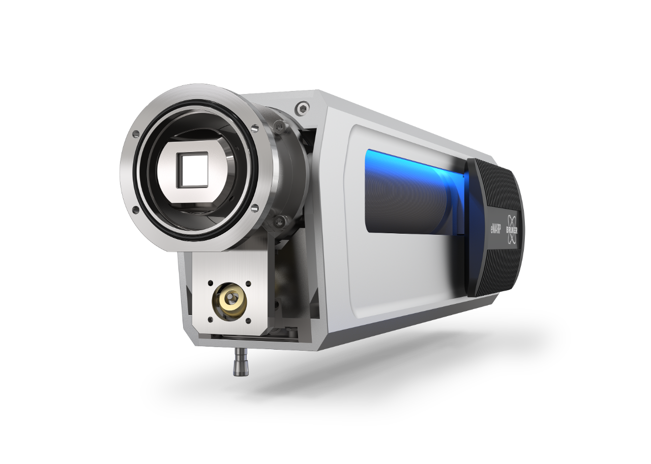
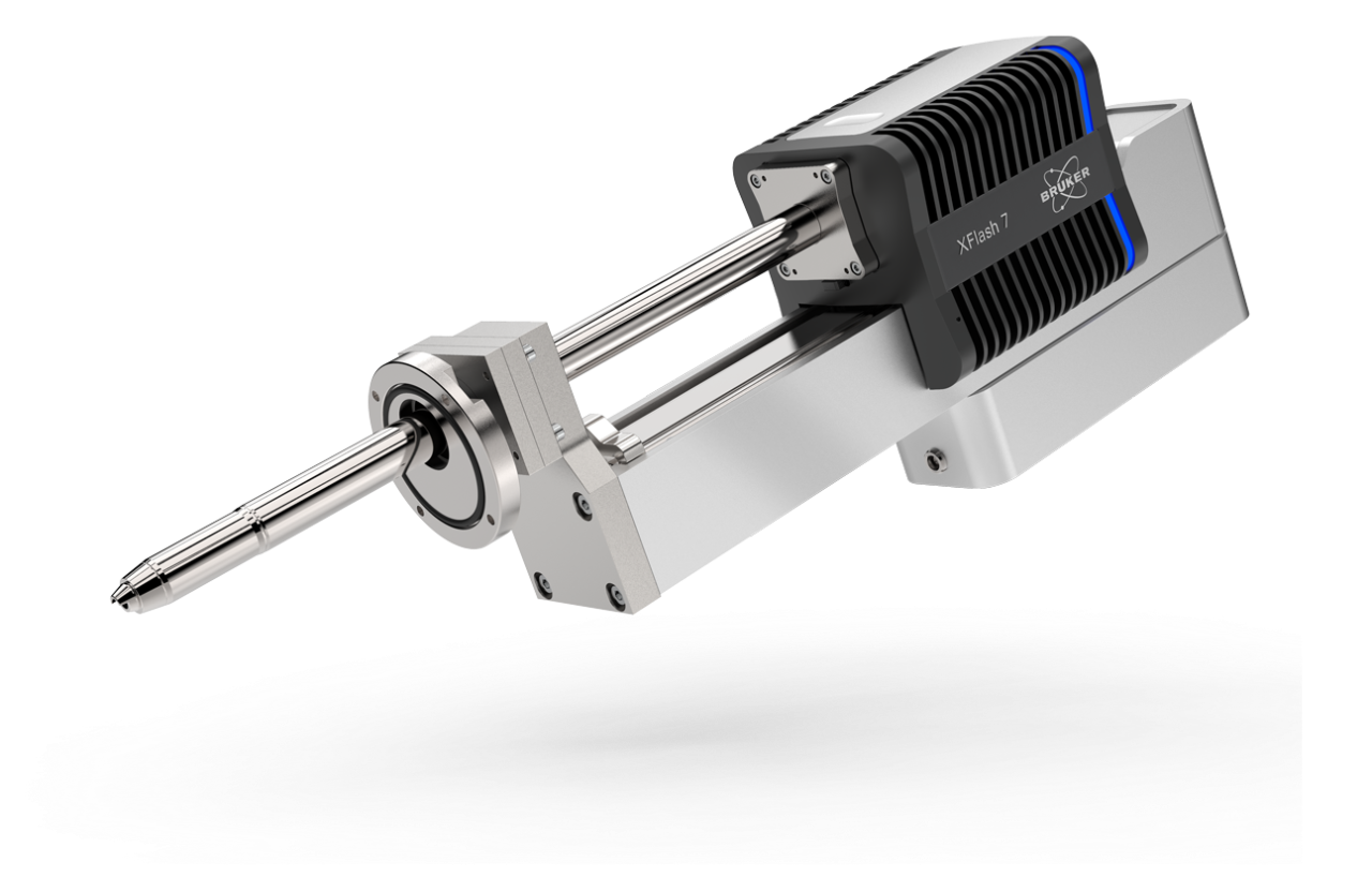
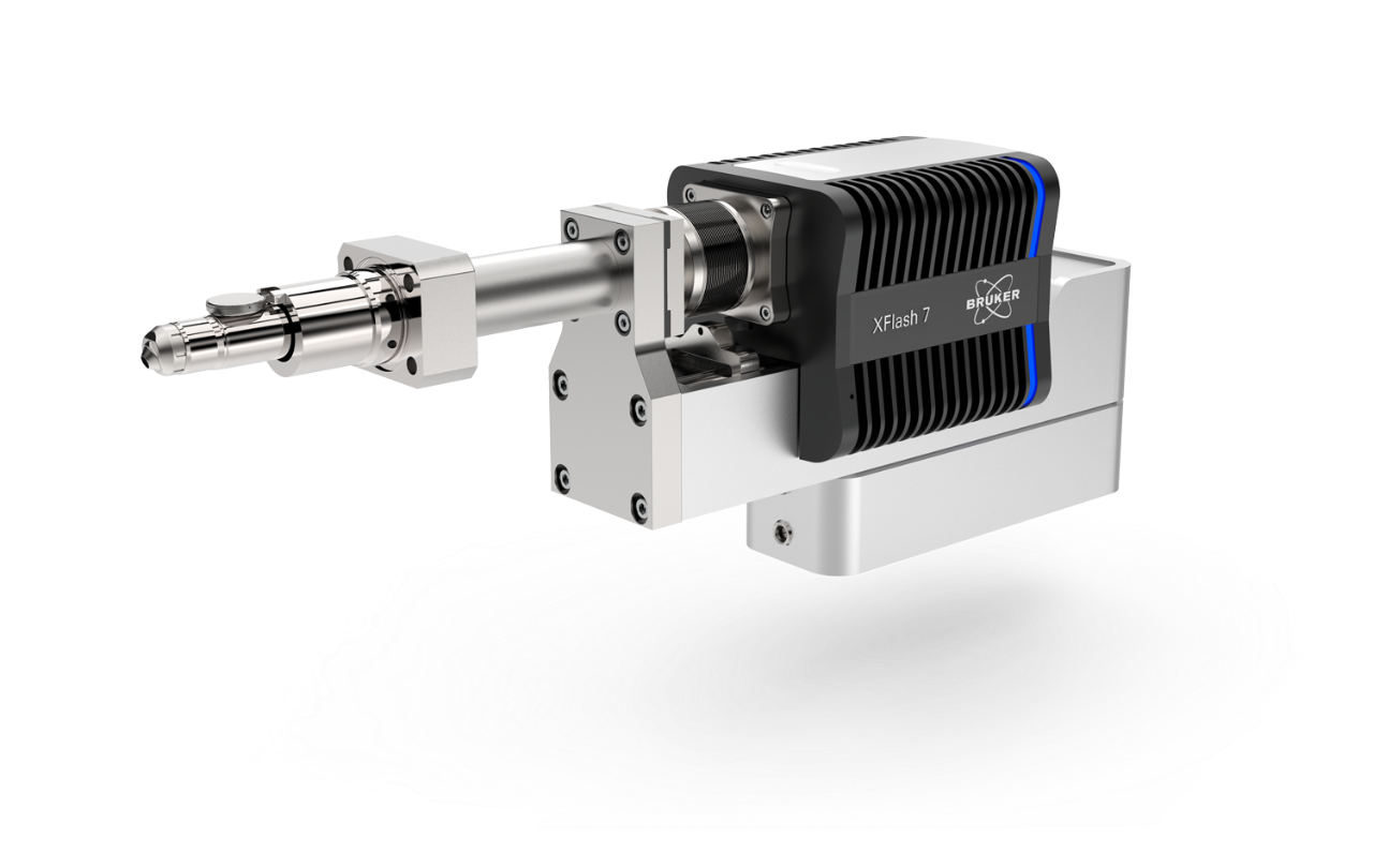
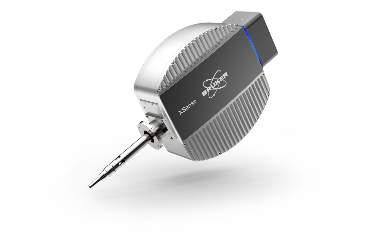
Surface metal contamination of semiconductor device affect its performance and product yields in multiple ways. For off-line inspection, Bruker offers SEM and TEM based solutions including Energy Dispersive X-ray Spectroscopy (EDS), Wavelength Dispersive X-ray Spectroscopy (WDS) and Electron Backscattered Diffraction (EBSD). These techniques allow localization, morphologic characterization and compositional analysis of individual contaminants. This can even be performed automatically using customized particle analysis software feature with ESPRIT software for EDS measurement.

Resolving Peak Overlaps in Semiconductor Tantalum Silicide

Since contaminants in semiconductor material are often small and thin features, the analysis is commonly carried out at very low acceleration voltages (1-5 kV). This limits X-ray spectroscopy to the low energy lines and requires analytical techniques with high spectral resolution capabilities such as WDS.