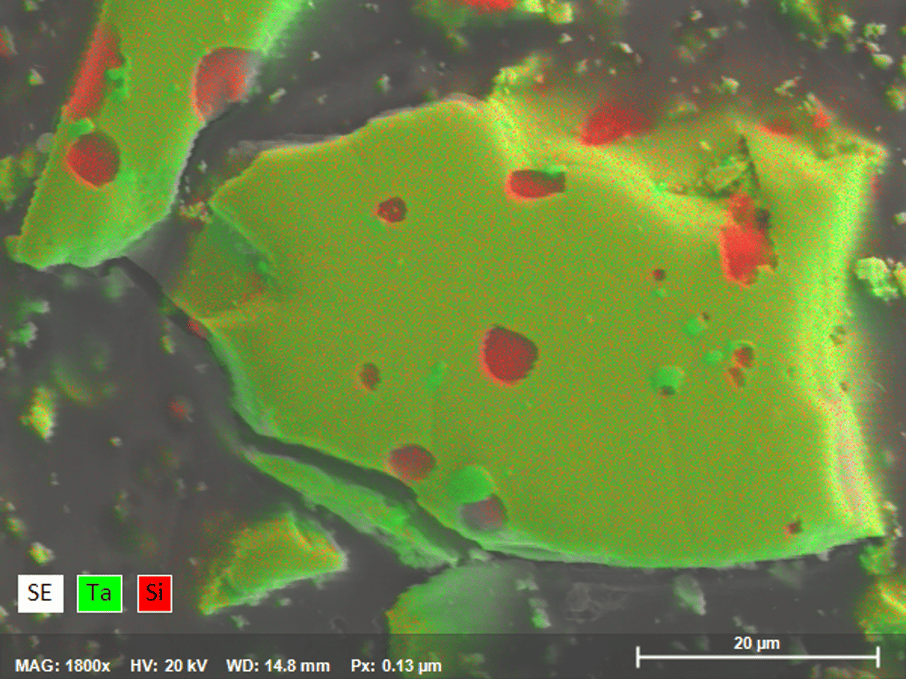
Resolving Peak Overlaps in Semiconductor Tantalum Silicide
Tantalum silicide is used for oxidation or temperature-resistant coatings, in microelectronics and optics. Tantalum silicide may also occur as refractory phase in semiconductor materials such as Si wafers.
In order to achieve a high spatial resolution during quality control, the analyses have to be carried out at low accelerating voltages, complicating the identification of minor phases. At low accelerating voltages, only the Ta M series energy lines are generated which severely overlap with the substrate Si Kα line.
The resulting EDS peaks of the primary elements are slightly broadened and masking the presence of the second element. By comparison, elements such as Ta are identified with confidence using QUANTAX WDS due to its superior peak resolution.

Alternatives to Wavelength Dispersive Spectroscopy
QUANTAX WDS is no longer available to purchase. However, we have suitable alternatives that cover the benefits of WDS - light element detection, peak deconvolution, trace element detection and efficient X-ray line separation.
To learn more about these solutions view our page Analytical Alternatives to Wavelength Dispersive Spectroscopy.
Information about the end of sales and service lifetime of QUANTAX WDS and XSense can be found here.