Failure Analysis
Failure Analysis
Failure analysis is an indispensable part of production control required in manufacturing semiconductor materials. Depending on the material and application, failure analysis can be divided into electrical, chemical, and mechanical tests, to investigate the root cause of a product or material failure.
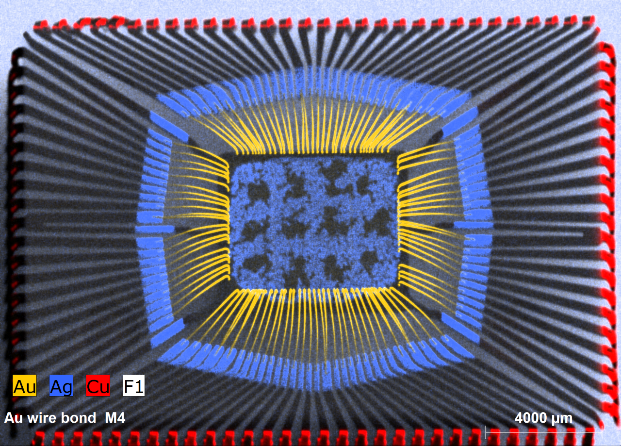
SEM/TEM-based Solutions
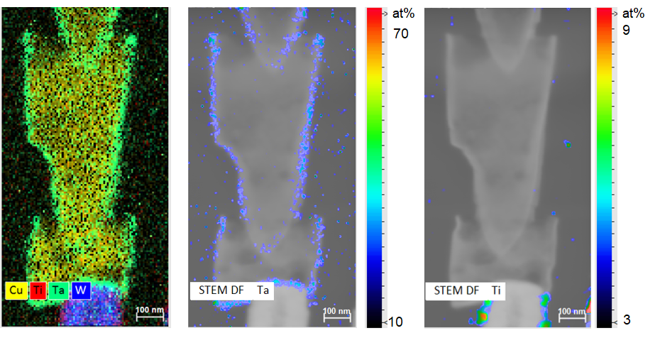
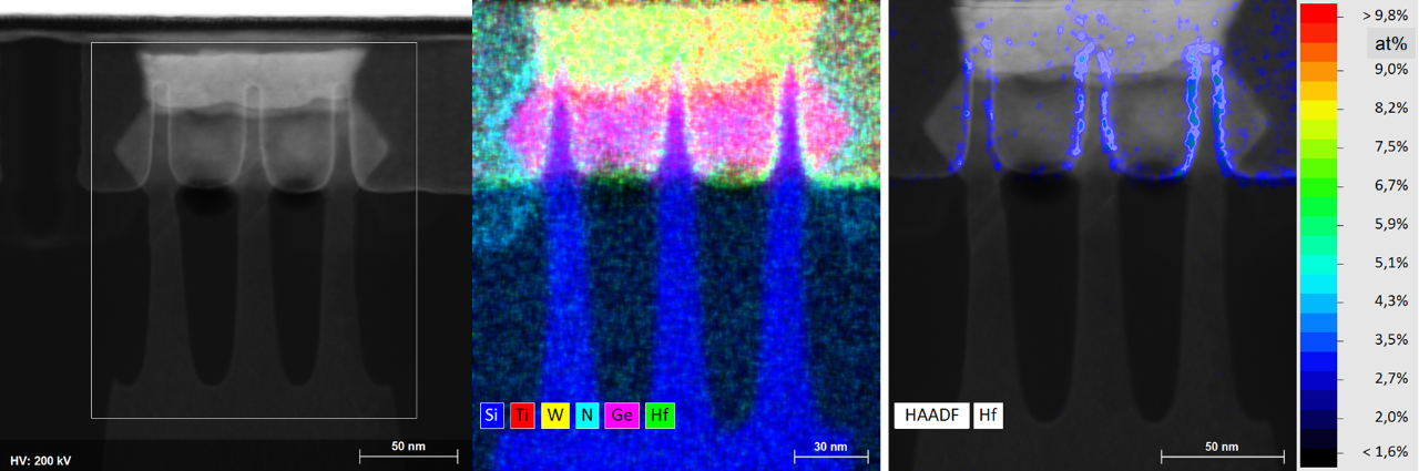
Quantitative EDS in STEM combined with individual sample preparation on the component level (FIB) provides the means to identify and study defects of the internal structure of semiconductor devices.
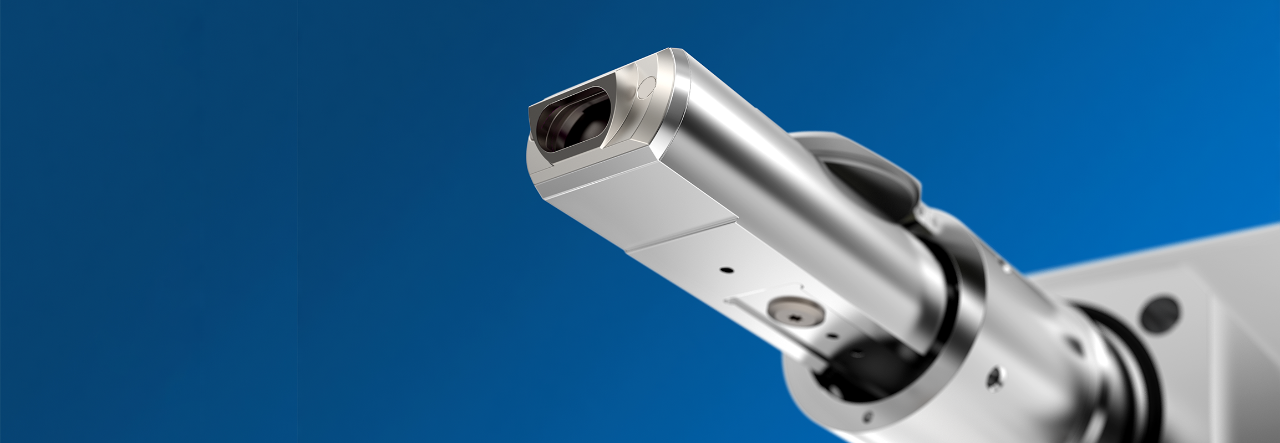
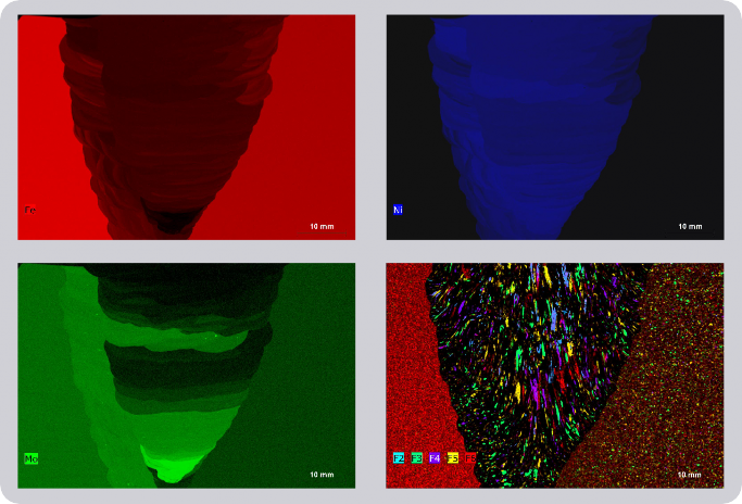
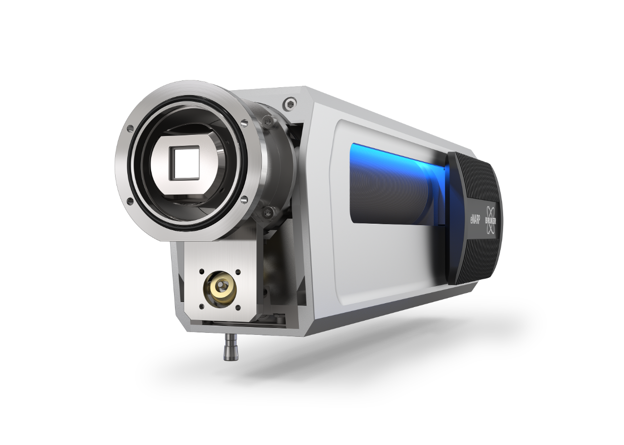
Micro-XRF
Allthough Bragg peaks are usually considered as hampering artefacts in micro-XRF, they are seen in spectra and thus can be visualized in XRF maps. Bruker's micro-XRF instruments enable the visualization of the appearance, disappearance or shift of such Bragg peaks with rapid large-area mapping. Revealing changes in the crystalline orientation or structure.
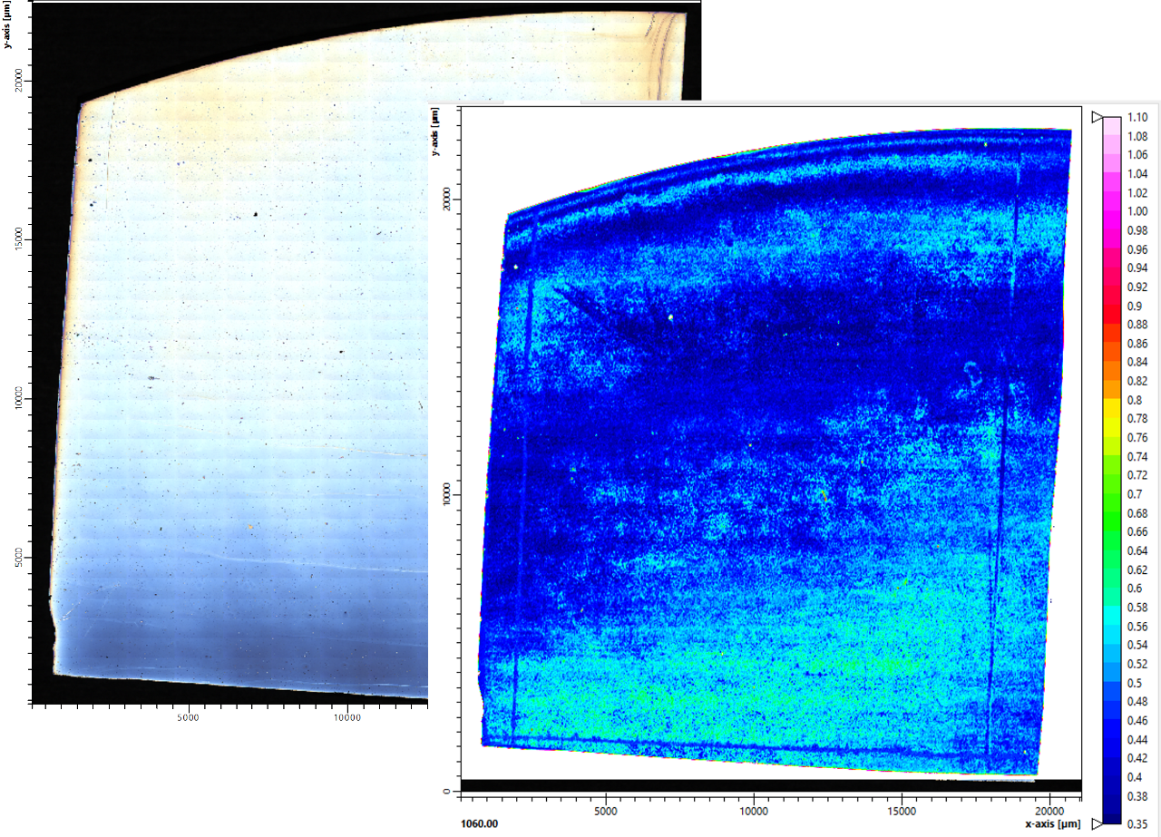
Infrared Laser Imaging (ILIM)
Infrared laser imaging is a powerful tool for non-invasive failure analysis in semiconductor manufacturing. In this example, an IR laser imaging analysis was performed on a plasma-coated wafer using the HYPERION II ILIM microscope to assess the uniformity of the coating.
By analyzing the single-wavenumber intensity, IR laser imaging provides a direct visualization of the coating homogeneity. This method helps manufacturers to:
- Optimize the coating process
- Identify potential defects
- Improve product reliability