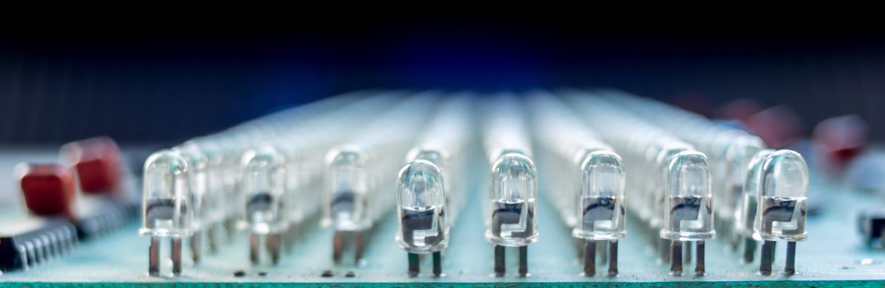

LCD Screens and Optoelectronics
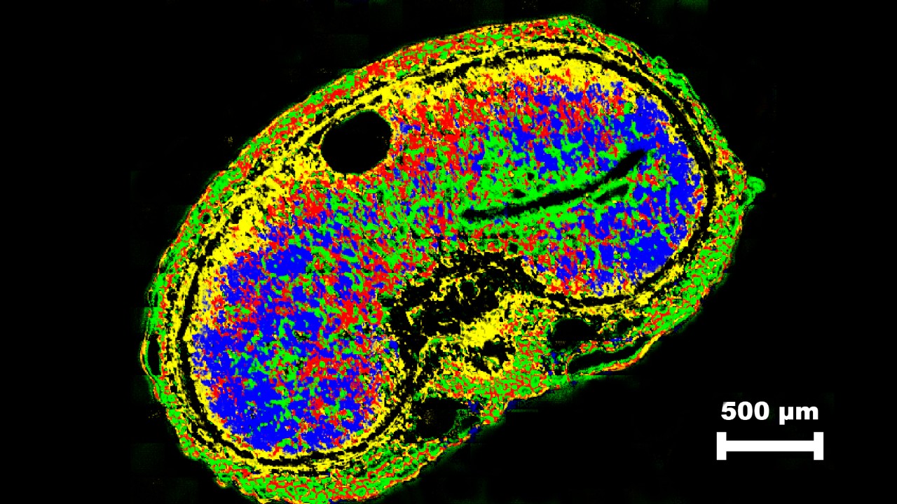
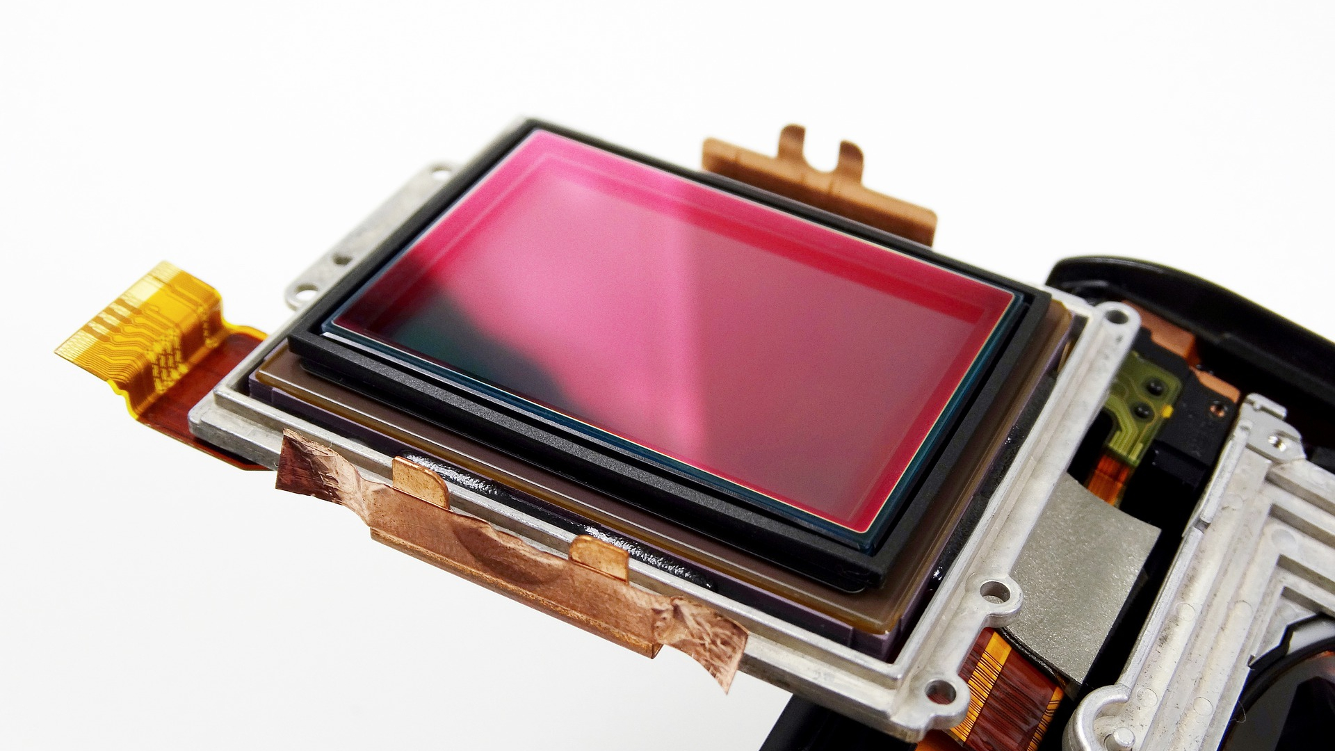
Defect Analysis of a CMOS Sensor by FT-IR Microscopy
The analysis of optoelectronic devices is quite complex since modern systems are highly miniaturized and composed of a multitude of materials. Especially the identification of microscopic contaminations is of particular interest as they can cause malfunctioning of the electronic device. Revealing the origin of the contamination and therefore allowing effective troubleshooting is one of the key applications of FT-IR microscopy.
It allows users to obtain an IR-spectrum of very small structures with a high lateral resolution, thereby revealing the chemical composition of an defined part of the sample. This makes FT-IR an indispensable tool for quality control and failure analysis of electronic sensors and other optoelectronics. It can help characterize defects, damages, contaminations and much more. It can even stimulate product development by characterizing infrared sensors.
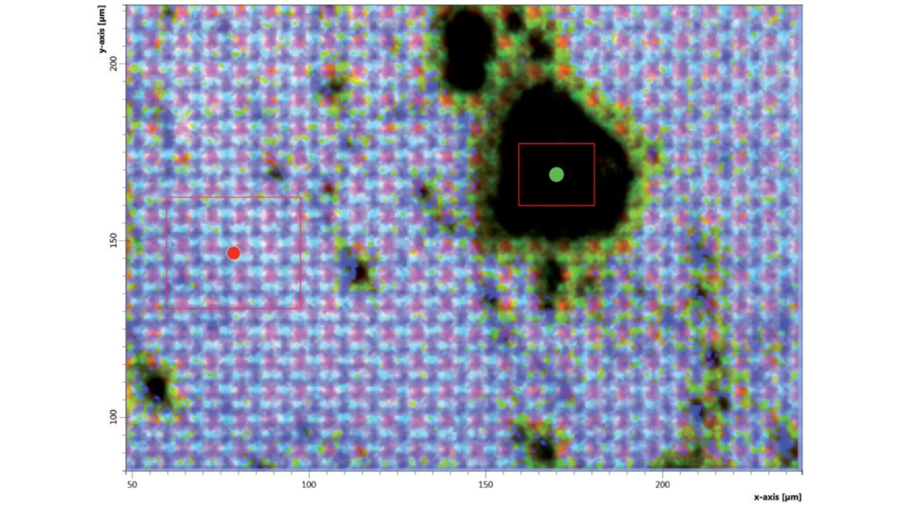
Investigate Contaminant Inside LCD Panel with Raman Microscopy
Displays, LEDs, LCDs and many more optoelectronical parts are laminated with protective layers of polymers or simply glued to glas surfaces. In both cases, meaning if the materials are transparent, confocal Raman microscopy has the power to look inside such assemblies.
Usually, very small contaminants like particles, fibers, dust and dirt are the culprits in such kinds of damages. Raman microscopy can not only find those microscopic impurities, it can identify them chemically to help discover the root cause of these product defects. Use it for damage analysis of:
- Screen and LCD assemblies
- Touchpanels
- Mounted sensors
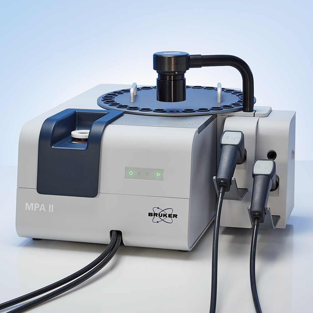
Sensor and Detector Characterization Using FT-IR
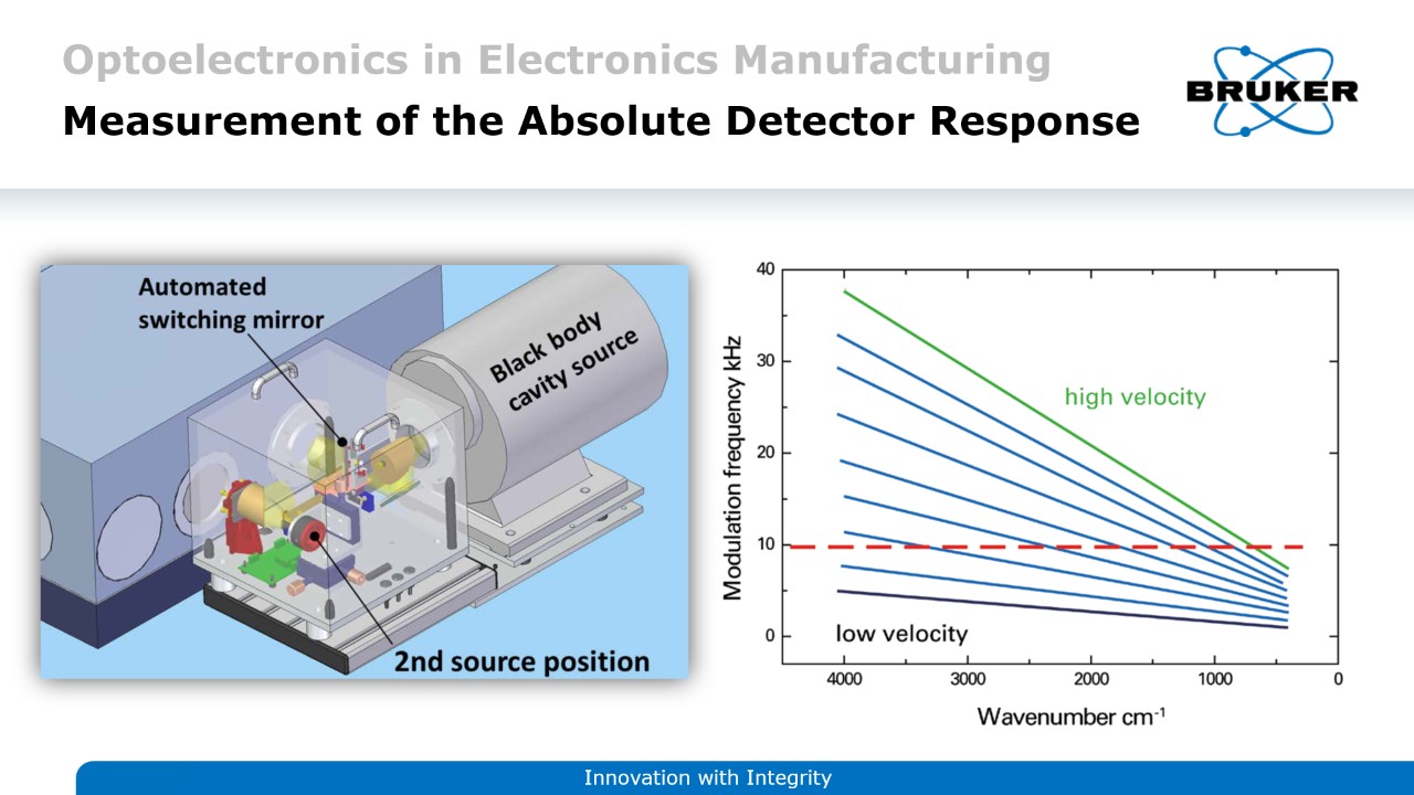
Detectors are everywhere nowadays - in smartphones, thermometers, cameras, light switches and many other devices. But before these detectors can start their work in our everyday life, they have to be thoroughly characterized and optimized.
This is exactly where an FT-IR spectrometer can be broadly applied, examining detectors for the three basic parameters:
- Spectral bandwidth of response (UV/VIS/IR/etc.)
- Radiant power needed for a response
- Sensor response time
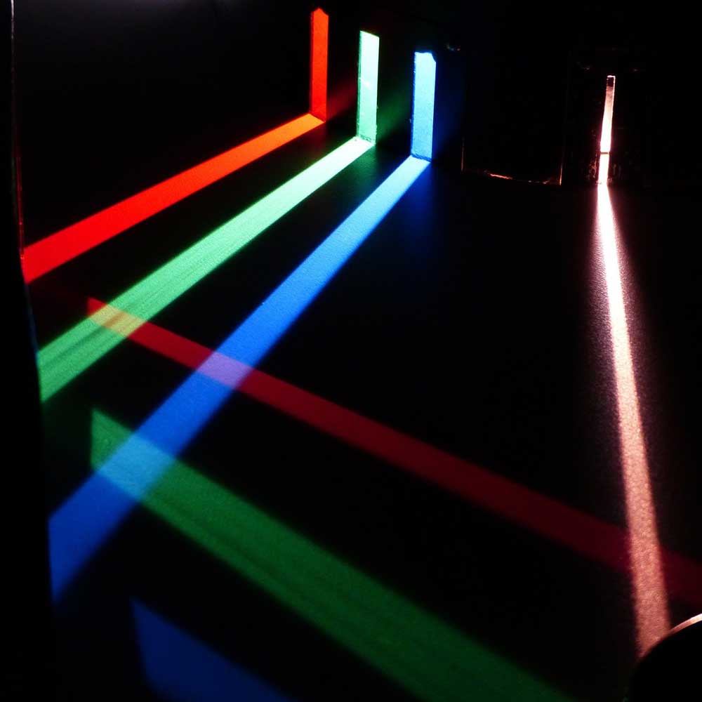
Applying FT-IR in the Development of VCSELs for Face Recognition

Vertical Cavity Surface Emitting Lasers (VCSEL) are a special type of semiconductor laser diodes which, unlike conventional edge-emitting laser diodes, emit perpendicular to the chip surface. This makes them easy to package as emitter arrays with hundreds of emitters on a single chip, which can then be placed in a smartphone (e.g. for face recognition).
In the analysis of VCSELs, FT-IR spectroscopy has proven to be a superior method compared to irradiance sensors and fast photodiodes. One of the many advantages is the possibility to determine emission spectra. Currently, research is focused on methods for characterizing VCSELs to support the theoretical modeling of VCSELs in basic research. You want to learn more?
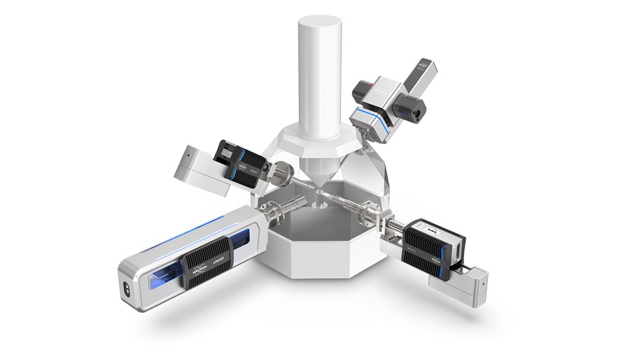
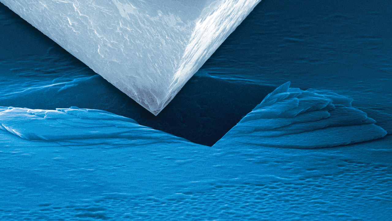
Correlating the Chemical Composition and Microstructure with Electrical and Optoelectronic Properties
Optoelectronic devices primarily rely on an optical stimulus to generate electrical pulses, and vice versa. They are commonly used as sensors or detectors in electronic devices.
SEM-based EDS and EBSD techniques are common analytical tools used in combination to investigate the correlation of the chemical composition and microstructure with optical, electrical and mechanical properties, and this down to the nanoscale. In-depth knowledge is possible with Bruker's advanced solutions for WDS, EDS, EBSD and TKD techniques to quantitatively measure the phase and orientation distributions. It allows, for instance, to investigate the effect of specific crystal orientation, strain and nature of grain or subgrain boundaries on the optoelectronic properties. In-situ correlation studies can also be conducted with Bruker's QUANTAX EBSD and Hysitron PI Series PicoIndenters.