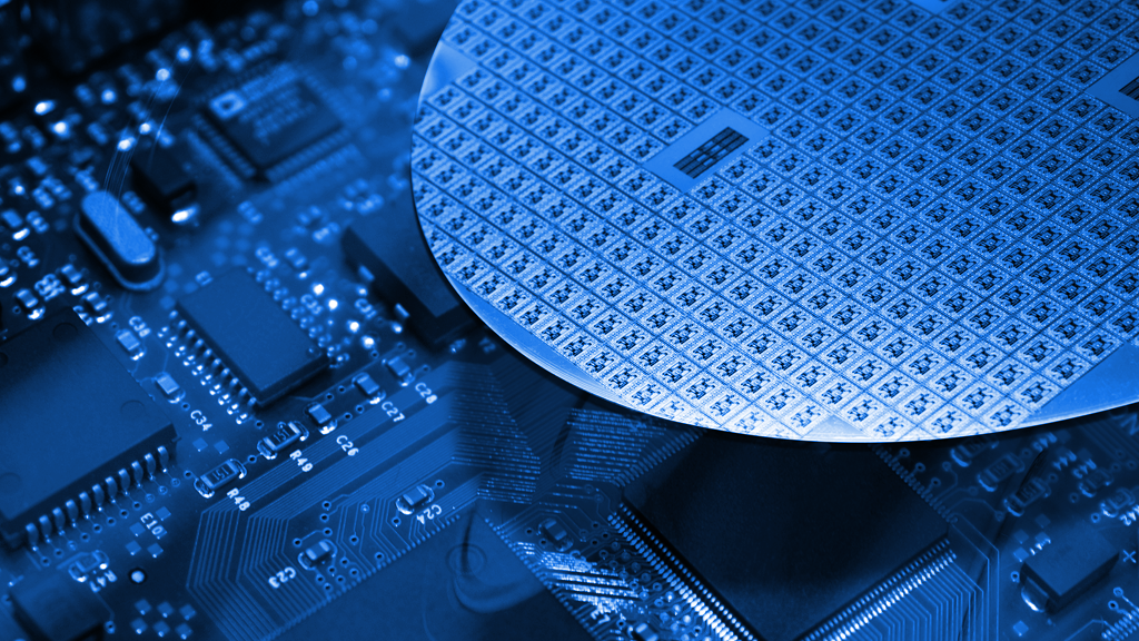
Thin Film Characterizations Applied in Semiconductor Industries
Discover the relevance of nanoindentation and nanoscratch methods for thin film property analysis
In this webinar, Dr. Pal-Jen Wei gives an overview of nanoindentation and nanoscratch characterization methods for thin films in the semiconductor industry.
Dr. Wei also provides specific examples in the following categories:
- Indentation-related applications investigating index of residual stress, index of dielectric constant, and indentation-induced delamination
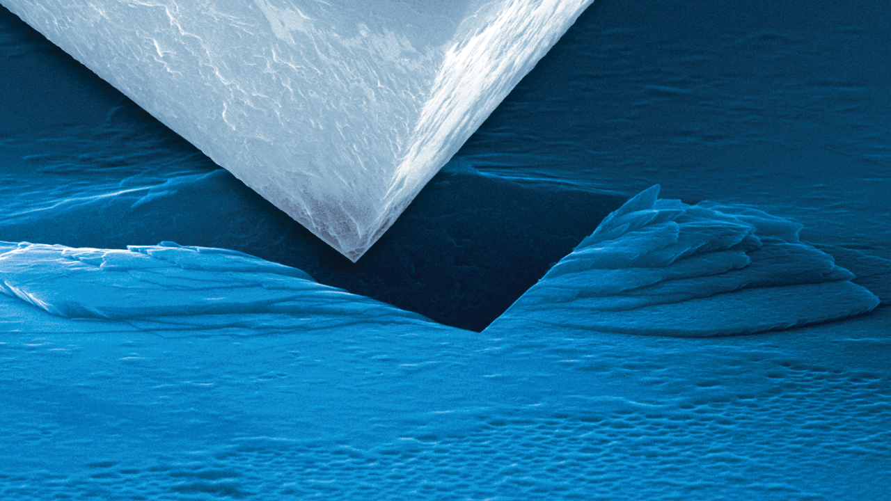
- Scratch-related applications measuring scratch-induced delamination and direct push of micro bumps from side wall
- High-temperature applications to study adhesion, glass transition temperature, and coefficient of thermal expansion
Webinar Summary
Advances in thin film deposition technologies and material development has enabled a wide range of industrial applications. Decreasing film thicknesses and material/manufacturing complexities pose increasing challenges for industrial engineers and process control in the evaluation of mechanical properties. Control of these ultra-thin films is extremely essential and presents a challenge in measuring mechanical properties with highly precise force, displacement, and positioning control.
This need to evaluate ultra-thin films has created a need for process grade metrology instrumentation with significantly enhanced precision in measuring a wide range of mechanical properties. Hardness, modulus, interfacial adhesion, fracture toughness, and temperature are just some of the mechanical property measurements that become significantly more difficult in thin films.
The webinar provides an overview of thin film characterizations applied in semiconductor industries using nanoindentation and nanoscratch techniques. Dr. Pal-Jen Wei introduces both the fundamental principles of the techniques and corresponding case studies.
Among the presented case studies are:
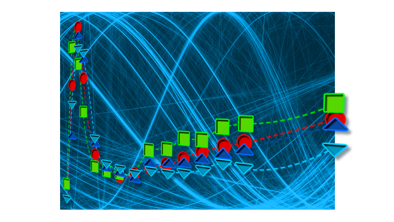
- Modulus mapping of a microchip to study copper grain orientation effects
- Indentation-based measurement of residual stress in silicon oxide films
- Glass transition temperature measurement in polymers using nanoDMA
Throughout the webinar, Dr. Wei emphasizes the advantages of the nanoindentation and nanoscratch techniques for thin film characterization, especially due to their high spatial resolution and ability to perform direct measurements on wafer surfaces.
Find out more about the technology featured in this webinar or our other solutions for Thin Film Characterization:
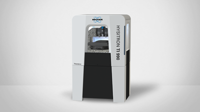
Featured Products and Technology

Speaker

Pal-Jen Wei, Ph.D.
Applications Scientist, Bruker
Dr. PJ Wei is an Application Scientist at Bruker Nano Surfaces, responsible for application development and technical support of Nano-Mechanical, Nano-Tribological and Nano-Indentation instruments. His academic background was in mechanical engineering and nano-metrology. Dr. Wei obtained his Ph.D. at National Cheng Kung University, Taiwan; majoring in nano-mechanical properties of thin solid films. Prior to joining Bruker, Dr. Wei was an Assistant Prof. at the Nanotechnology and Micro-system Institute in Taiwan and then a senior engineer of RD department in Catcher Tech. He has published in over 30 peer reviewed international journal papers and has also presented at many international conferences.