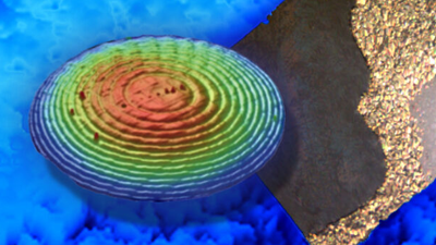
Measuring Profile and Real Mean Roughness with 3D WLI Profilers
Producing next-generation materials and manufacturing them at scale requires fast, accurate mean surface roughness evaluation.
This webinar focuses on the practical impacts and differences between stylus and areal methods of assessing mean roughness (Ra), as well as the key considerations necessary for determining the most appropriate applications for either method.
The full-length recording of this webinar is featured in our 3D Surface Measurement Knowledge Pack.
Webinar Summary
Assess mean surface roughness by profile and areal methods
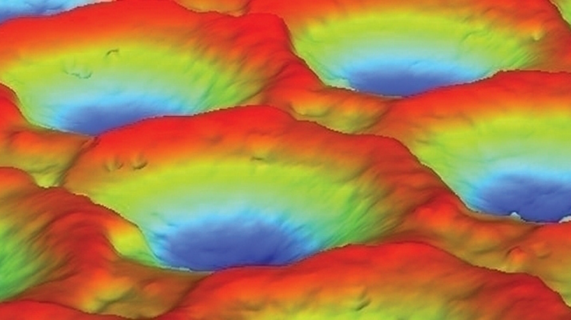
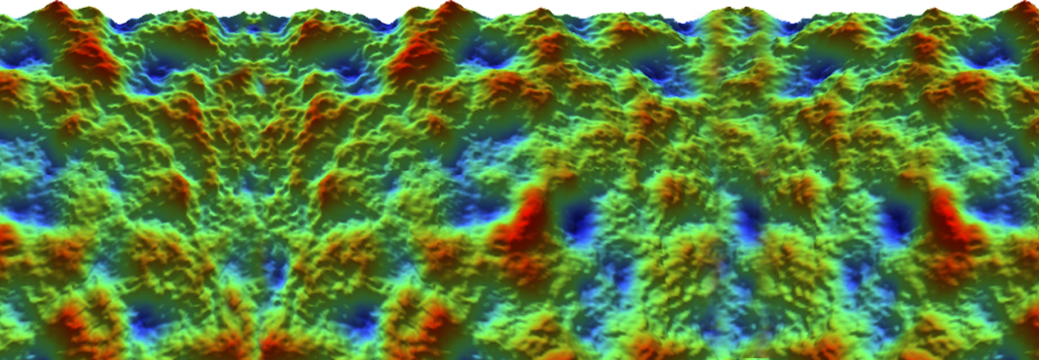
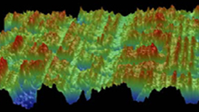
Stylus-based profilers have long been used to capture mean roughness (Ra) and to assess product and process quality. However, modern engineering and manufacturing often generate random and/or complex engineered surface textures that are difficult to assess with a single-line profile.
Consequently, though mean roughness can easily be captured through one—or a few—profiles for standard manufacturing processes (those which leave a single texture orientation), optical areal measurement becomes mandatory to properly evaluate the surface in many cases.
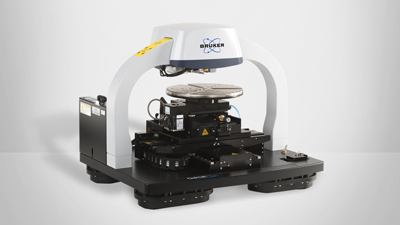
This webinar aims to provide both theoretical background and practical measurement considerations (including filter selection, measurement setup, and data processing) for measuring profile and real mean roughness using Bruker's Stylus and Optical profilometry solutions, highlighting the ways that both profile and areal methods are able to co-exist in modern industry.
This webinar was presented on April 06, 2020.
SEE RELATED RESOURCES:

Featured Products and Technology
Speakers

Samuel Lesko, Ph.D.
Dir. of Technology and Apps Development for Tribology, Stylus & Optical Profilers, Bruker
Samuel Lesko has over 20 years of optical and stylus profiler applications experience, particularly in using white-light interferometry in a wide variety of fields, from MEMS and semiconductor to automotive and aerospace. He is a member of SME and part of ISO/TC 213/WG committee (areal roughness) and obtained his physics Ph.D. and material science engineering degree at the University of Burgundy in France.

Ian Armstrong, Ph.D., Senior Manager AFM Probes, Bruker
Ian Armstrong has worked at Bruker for over 16 years in various roles from applications to product management. He is currently senior manager of Bruker's AFM probes business unit.