
Thin Film Interface Adhesion Characterization for Industrial Applications
Learn how to collect high-confidence thin film adhesion measurements via nanoindentation and nanoscratch testing
Product innovation in modern industries—especially the semiconductor, hard coating, and display industries—relies heavily on decreasing the thickness of thin-film components.
We are pleased to present this webinar as one part of our 4-part Thin Film Measurements Series, in which our experts provide the information manufacturers need about leading-edge nanomechanical testing technology for thin films measurement, complete with use case studies for a range of industrial applications.
Collect High-Confidence Adhesion Measurements
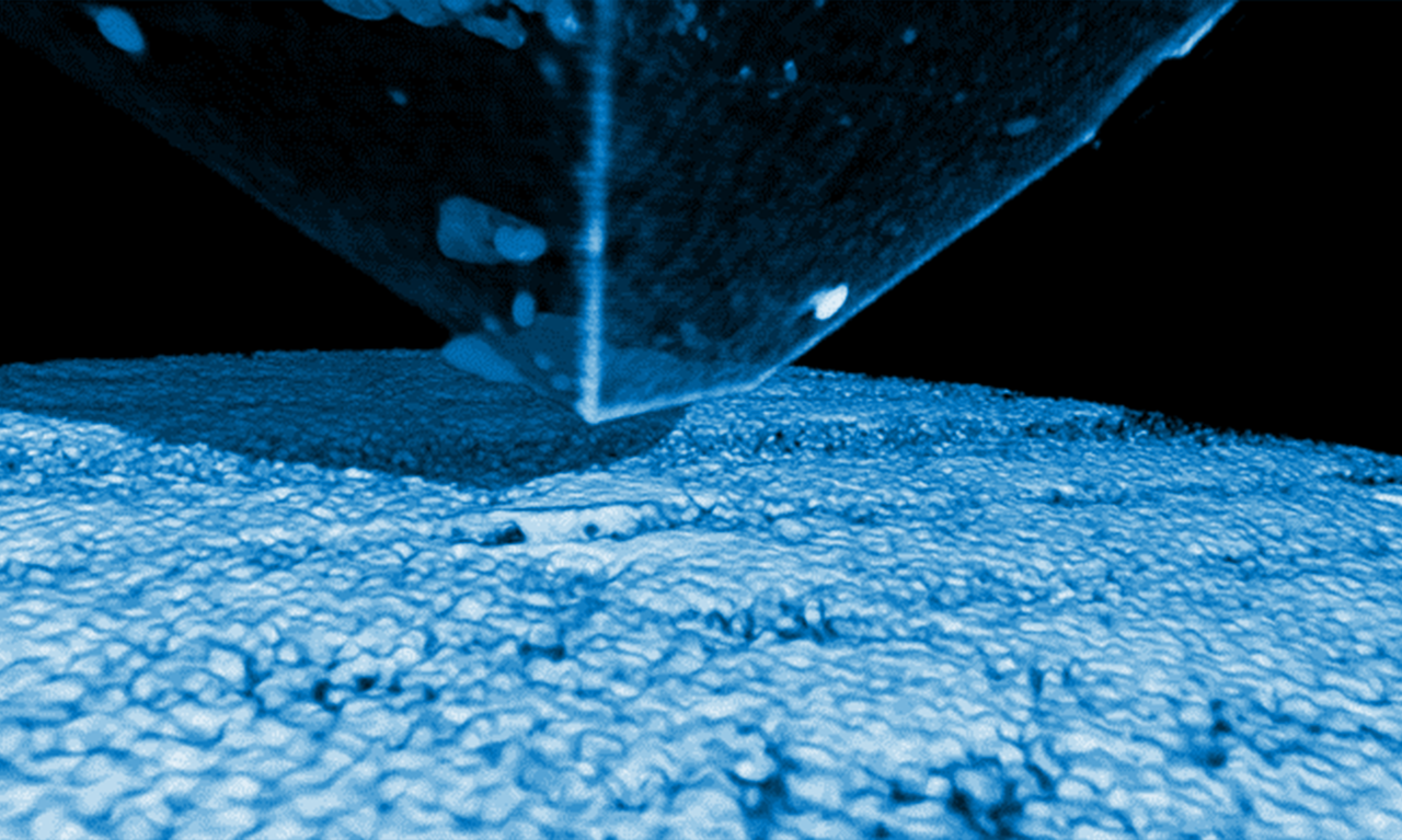
The widespread use of porous low-dielectric constant materials has rendered previous large-scale interface adhesion measurement technology obsolete in a very short period of time. At the same time (and ever since) nano-scratch techniques have progressively emerged as the only nano-scale thin film adhesion measurement solution for in-situ observations and quantitative measurements of film adhesion. This has led to the large-scale adoption of nanoscratch and nanoindentation testing of porous low-dielectric constant materials as an in-line monitoring tool in multiple industries ranging from semiconductor to hard coating to display and anti-corrosion film industries. In this webinar, you can expect to:
- Understand the challenges researchers face when measuring the adhesion of thin films.
- Find out how nanoindentation and nanoscratch testing supports in-line process innovation.
- Identify and analyze the correlation between nanoindentation and nanoscratch test results.
- Get practical guidance for using indentation-induced delamination to overcome the challenges posed by rough samples and high temperatures.
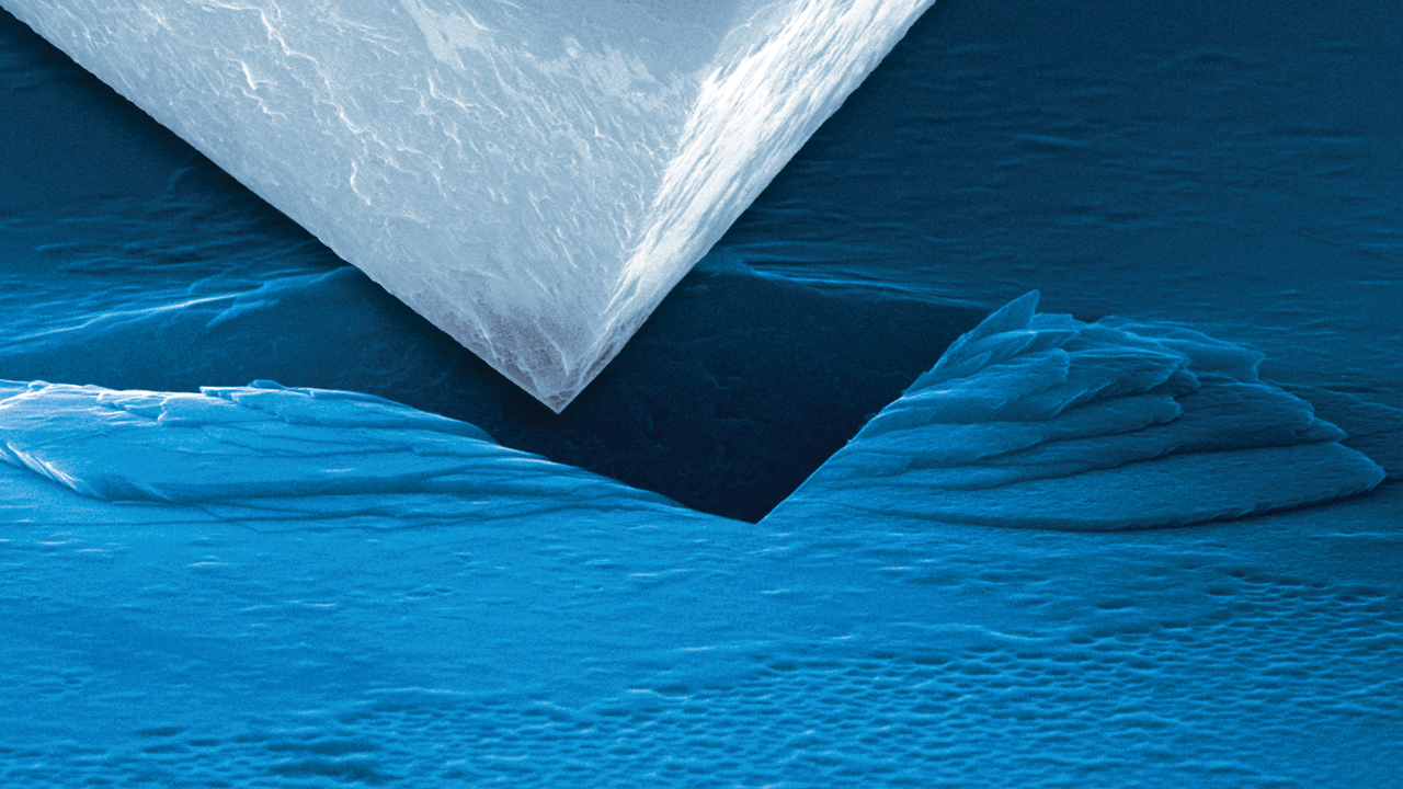
This presentation focuses on explaining the concepts and applications of thin film interface adhesion and the complexities of direct imaging of nanoscratch and nanoindentation tests with a scanning electron microscope.
Find out more about the technology featured in this webinar or our other solutions for Thin Film Interface Adhesion Characterization:


Speaker

Pal-Jen Wei, Ph.D.
Applications Scientist, Bruker
Dr. PJ Wei is an Application Scientist at Bruker Nano Surfaces, responsible for application development and technical support of Nano-Mechanical, Nano-Tribological and Nano-Indentation instruments. His academic background was in mechanical engineering and nano-metrology. Dr. Wei obtained his Ph.D. at National Cheng Kung University, Taiwan; majoring in nano-mechanical properties of thin solid films. Prior to joining Bruker, Dr. Wei was an Assistant Prof. at the Nanotechnology and Micro-system Institute in Taiwan and then a senior engineer of RD department in Catcher Tech. He has published in over 30 peer reviewed international journal papers and has also presented at many international conferences.
Thin Film Measurement Webinar Series Sessions
Part 1

Part 3
Part 4
