EDS Mapping Fundamentals: Achieving High-Quality EDS Maps in SEM
What to expect
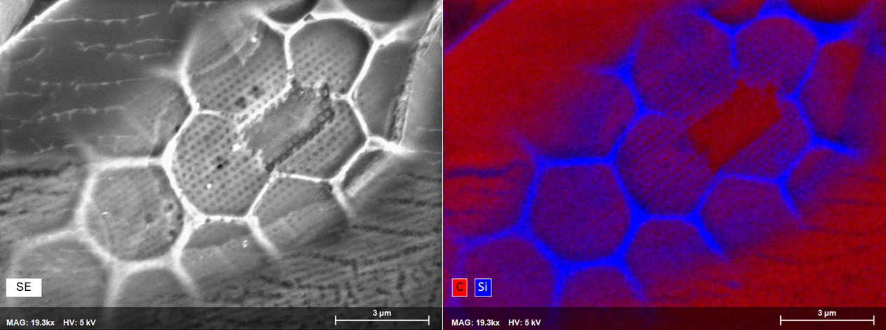
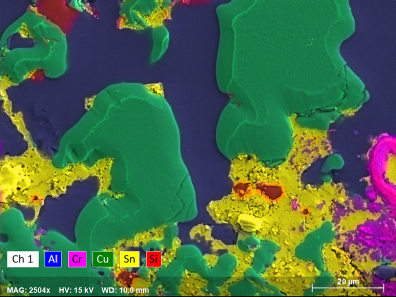
Energy Dispersive Spectroscopy (EDS) in Scanning Electron Microscopy (SEM) is a versatile and powerful, non-destructive analytical technique for fast, high-resolution elemental mapping. While SEM EDS is widely adopted for industrial and academic research, users often run into real challenges such as noisy map results despite good SEM images; or low x-ray counts, charging effects, misidentified elements, shadowing, and poor spatial resolution.
This webinar intends to address these issues in details and to provide users with realistic strategies to systematically achieve high quality EDS mapping.
Attendees will learn how to:
- Evaluate the quality of EDS map data with confidence
- Recognize common pitfalls and understand their root causes
- Apply smart, practical methods to optimize SEM and EDS settings for any material/sample

Who should attend
- Researchers and lab managers in Academia and Industry working with analytical microanalysis.
- Experienced analysts who wish to optimize their EDS mapping workflows.
- Materials and industry experts across diverse market segments such as Material Sciences, Battery, Life Science, Forensics, Geology, Semiconductor etc., where high quality SEM EDS mapping is essential.
Speakers

Dr. Purvesh Soni
Sr. Applications Scientist EDS, Bruker Electron Microscope Analyzers
Watch this On-Demand Webinar
Please enter your details below to gain on-demand access to this webinar.