Fast Elemental Mapping of Si and W Wafer Etching Residues
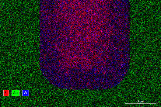
SEM elemental mapping with high input count rates (ICR) is desirable when analysis time should be minimized. When using typical input count rates (in this example 63 kcps) at short measurement times (1 frame = 7 seconds), the number of total counts is too low to provide quantitative element distributions or even to reveal the distribution without filtering (Figure 2 top).
Fast elemental mapping is especially challenging when peak deconvolution is required, like in this example with Si-K and W-M peak line series overlaps (i.e., Si-Ka at 1.740 keV and W-Ma lines at 1.775 keV). An online deconvolution function is applied to the EDS mapping to retrieve the deconvolved net peak intensities (Figure 1).
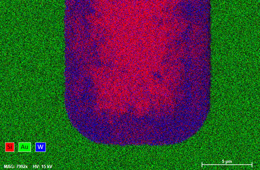
Higher electron beam currents provide higher incoming count rates (ICR in this example 700 kcps) allowing fast elemental mapping with sufficient count statistics and preserved spectral quality. Using such measurement conditions, the new XFlash® 7 detectors provide a detailed element distribution image down to physically optimal resolution without the need for map filtering (Figures 2 bottom, 3 bottom).