Thin Film Stress Measurement Using Dektak Stylus Profilers
Stress Measurement Analysis with Dektak Stylus Profilers
Accurate assessment of the deformation caused by film stress is critical for developing controllable processes and producing high-quality devices. The optional Stress Measurement Analysis software for Dektak stylus profilers affords the flexibility to accurately characterize film stress, as well as roughness and steps, for comprehensive film analysis on a single platform.
This technical note discusses stress measurement methodology, the algorithms behind the Dektak Stress Measurement Analysis, and important considerations for achieving accurate stress calculations.
Readers can expect to learn more about:
- How the Dektak Stress Measurement Analysis software allows for accurate assessments of film stress for process control in the manufacture of semiconductors, MEMS, thin film filters and other devices
- Practical guidance for using the Dektak Stress Measurement Analysis software, including establishing scan parameters, radial map setup, and data analysis.
KEYWORDS: Pre-deposition stress; post-deposition stress; residual stress measurement; topography; wafer bow

Accurate assessment of the deformation caused by film stress is critical for developing controllable processes and producing high-quality devices. This technical note discusses stress measurement methodology, the algorithms behind the Dektak Stress Measurement Analysis, and important considerations for achieving accurate stress calculations.
Stress is generated in both the substrate and film during deposition and planarization processes employed in the manufacture of semiconductors, MEMS, thin film filters and other devices. Excessive film stresses can lead to deformation, cracking, delamination, shorts, and other failures that can render a device unusable. Stress Measurement Analysis, an optional software package for Dektak® stylus profilers, calculates tensile and compressive stresses then displays the results, allowing for accurate film stress assessments for process control.
Measurement Theory
The standard stress measurement technique is straightforward: the curvature of the substrate is measured prior to deposition, then the substrate is measured along the same trace after a film is applied. Stress Measurement Analysis uses the bending plate method to calculate stress in a deposited thin film layer, based upon the change in curvature and material properties of the film and substrate.1,2 The key parameters needed for the stress calculation are the substrate’s radius of curvature (R) before and after deposition. If the height of the substrate is expressed as a continuous function of distance along the substrate, y = f(x), then the radius of curvature at any point may be calculated as:

Assuming an initially flat substrate, the stress in the film can then be calculated as:

σ - Stress in the film, after deposition
Rpre - Substrate radius of curvature, before deposition
Rpost - Substrate radius of curvature, after deposition
𝐸 - Young's modulus
ν - Poisson's ratiot
ts - Substrate thickness
tf - Film thickmess
Each scan is fit with a 5th order polynomial by the method of least squares. The fit to each scan is then differentiated to produce the function y’(x) and again to produce y”(x).
These functions are substituted into Equation 1 to calculate the radius of curvature as a function of scan position before and after deposition. The two radii are substituted into Equation 2 to calculate pre-deposition and post-deposition stress. The difference between these values is the film-induced stress. Negative values of stress are compressive (convex surface); positive values are tensile (concave surface). Stress is measured in units of Pascal (N/m2).
Radial Map for Alignment
Accurate stress measurement requires scans across a significant portion of the center of the substrate, typically 90% of total diameter, and the pre- and post-deposition scans must represent the same orientation of the wafer. Radial Map is a capability that allows the user to measure the shape of a wafer or any round substrate up to 300 mm.
Radial Map consists of measuring multiple profiles at incremental theta angles: from one edge to the opposite edge of wafer/substrate, passing through its center. All these individual profiles are then bundled together with the same common height value of zero at the center prior to interpolation, as seen in Figure 1. Since using Radial Map for stress requires measurements over large ranges to determine shape and form, a large 12.5 µm stylus radius is recommended.
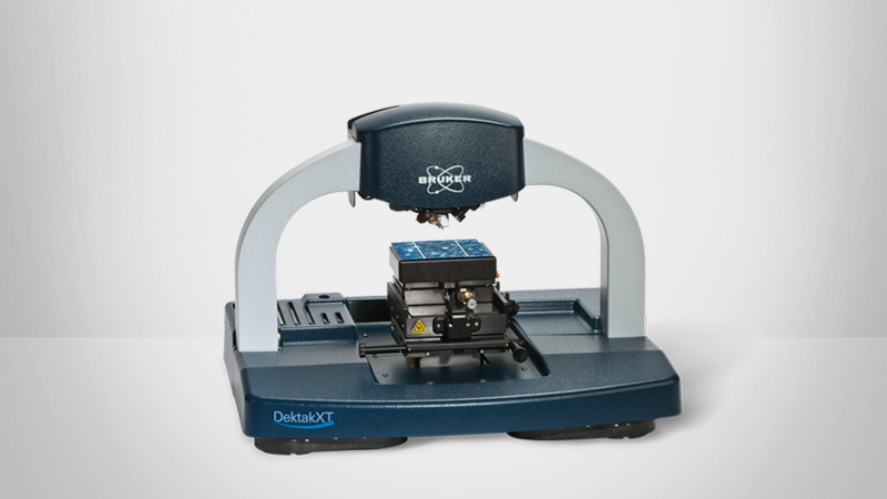
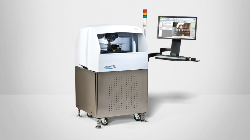
While stress can be measured using any Dektak profiler with the Stress Measurement Analysis installed, the Bruker Dektak stylus profiler is the recommended instrument, due to its long-range scanning capability (up to 200 mm/300 mm), 3-point suspension stage, and optional programmable theta positioning.

Conducting a Stress Radial Measurement
Wafer placement and rotation
- Place wafer directly on the wafer chuck. It is important to properly center the wafer on the chuc for best measurement results. Be sure to use the proper set of centering screw stops on equipped chucks for the wafer diameter being measured by placing the wafer against them for repeated proper wafer centering. Make note of the notch or flat location for pre- and post-process measurement.
- Level the wafer using the front level adjust when measuring a scan front to back and the left level adjust when measuring a scan left to right on the sample. Repeat the two leveling adjustments until the two raw scans are within +/- 20 µm in slope.
Measurement scan setup parameters
Recommended measurement scan parameter defaults are shown in Figure 2.
- Scan type uses Standard Scan to track the surface.
- Z range of 1 mm is usually sufficient unless there is extensive wafer bowing.
- Profile type is Hill and Valleys to follow wafer form up and down.
- The recommended stylus type is the 12.5 µm tip radius.
- Stylus Force should be set to a maximum of 15 mg for the 12.5 µm stylus on a bare wafer and should be lower if a smaller stylus is used. For soft-material films, reduce the force to eliminate potential damage at high scan speeds.
- Measure length is the scan length for the full wafer diameter. If the length exceeds the Dektak model scan length, the software will automatically enable a stitching option to perform multiple scan measurements and stitch them together.
- Duration is automatically determined, and it is recommended that the user not change this parameter. Duration determines the speed, resolution, and sample points for the best measurement results.


Radial Map setup and capture
The Radial Map parameter setup window is shown in Figure 3.
- Theta Extent: 360° covers the full shape while 180° and 90° respectively cover half and one quarter of the sample. This value is typically set to 360°.
- Theta Resolution is the angular distance between each profile around the wafer and is synchronized with the Number of Diameter Traces, with the minimum angle being 1°.
- Number of Diameter Traces is the number of profiles across the center of the wafer, with the maximum being 180.
- Scan Offset should remain and 0 and Re-null Tower to No.
For precise software wafer centering click on button to launch Part Center Location. Follow instructions from this window using the XY stage to move and center the red fiducial on the wafer border at the requested locations. While there is inherent freedom to choose location versus what the software requests, it is critical to sustain precise edge positioning on the sample edge.
All radial map measurements must start from the center position. To recover this important position, conveniently click on Move to Center.
Once the setup is complete, press Measurement. The initial profile will be from wafer center to front edge, followed by the acquisition of the full wafer profile that includes some iterations in case stitching is required.
Analyzing results
Topography: Once the radial map is acquired, the system conveniently adds and displays the Wafer Bow analyzer. This Analyzer displays the color map of the acquired data along with the highest and lowest datapoint parameters, as seen in Figure 4. Other standard software analyses can be applied to this dataset.
Stress: By measuring full wafer topography before and after thin film deposition, it is possible to measure residual stress in the deposited film through change of local curvatures. The stress calculation process is straightforward by opening the radial map from a wafer after film deposition then adding Stress Analysis.


Right-Click on Stress to Edit Settings. In the Stress Parameters window, use the Editor option to select substrate and film composition from the many materials available, thus obtaining elasticity constant as seen in Figure 5.
Then, indicate thickness for substrate and film in micron units. Indicate thickness for substrate and film in micron units. Finally, select the radial map from wafer before deposition and click OK to launch stress calculation as seen in Figure 6. Many other statistical analyses can also be obtained as seen in Figure 7.


Note, the measured values of Young’s Modulus and Poisson’s Ratio vary considerably from source to source depending on measurement method. For silicon in the <100> and <111> orientations, Dektak’s stress calculation software uses the values measured by Brantley.3
Conclusion
Accurate stress measurement helps process developers avoid nonplanarity effects to ensure uniform deposition and high part performance for samples up to 300 mm in diameter, 1 mm Z range with the largest force range from 0.03 to 15 mg. The Stress Measurement Analysis option for Dektak stylus profilers affords the flexibility to accurately characterize film stress, as well as roughness and steps, for comprehensive film analysis on a single platform.
References
- Stoney, G. (1909). The tension of metallic films deposited by electrolysis. Proceedings of the Royal Society of London. Series A, Containing Papers of a Mathematical and Physical Character, 82 (553), 172–175. https://doi.org/10.1098/rspa.1909.0021
- Jaccodine, R. J., Schlegel, W. A. (1966). Measurement of Strains at Si-SiO2 Interface. Journal of Applied Physics, 37 (6), 2429–2434. https://doi. org/10.1063/1.1708831
- Brantley, W. A. (1973). Calculated elastic constants for stress problems associated with semiconductor devices. Journal of Applied Physics, 44 (1), 534–535. https://doi.org/10.1063/1.1661935
©2022 Bruker Corporation. All other trademarks are the property of their respective companies. All rights reserved. TN504, Rev. A0.
Download the Full-Length PDF
This resource is included in our Stylus Profiler-Based Characterization of Thin Films knowledge pack.
Get instant access to all app notes, webinars and lectures, and technical demonstrations on using stylus profilometry for thin film characterization, all in one place.
