
Latest Advances in Scanning Microwave Impedance Microscopy (SMIM)
Gain new insight into the applications of sMIM mode and its advanced implementations on Bruker AFM systems.
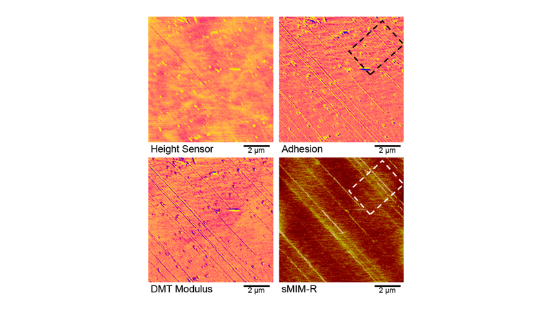
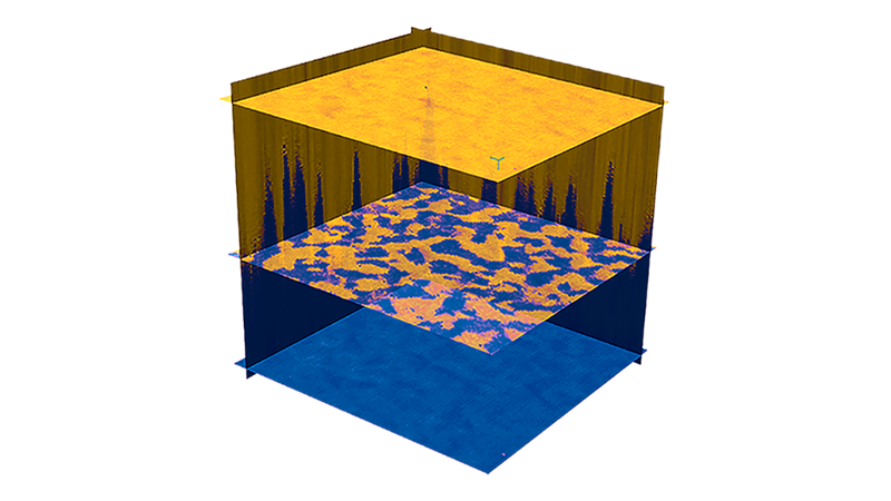
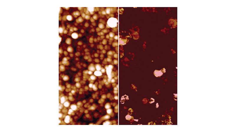
This webinar explores several case studies to illustrate how the sMIM method can be applied to a wide variety of samples such as 1D & 2D materials, ferro-electrics, dielectrics, and semiconductors.
Learn More About Nanoelectrical Characterization
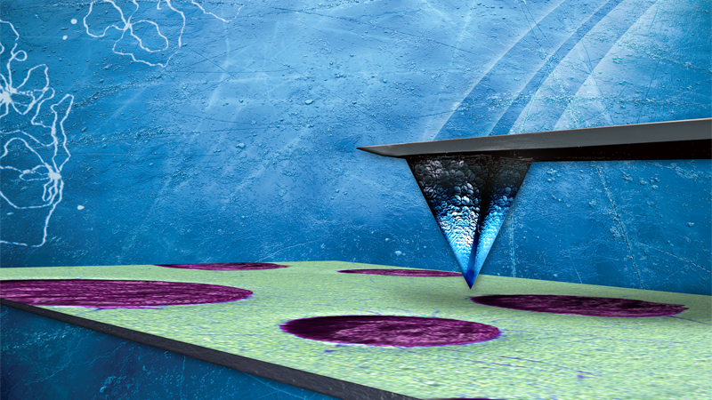
We are pleased to invite you to join the next atomic force microscopy webinar, "Latest Advances in Scanning Microwave Impedance Microscopy," with guest speaker Nicholas Antoniou (PrimeNano, Inc.). Scanning Microwave Impedance Microscopy (sMIM) is a Scanning Probe Microscopy (SPM) method based on a near-field microwave imaging technique for the characterization of local variations in permittivity and conductivity of materials with nanoscale spatial resolution.
The presentation will include several case studies, including:
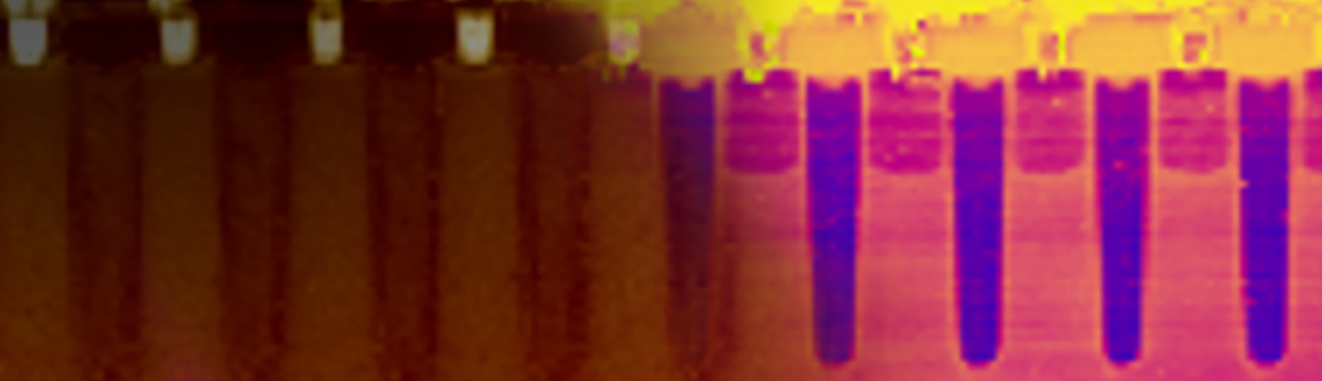
- 2D carrier profiling of semiconductor devices;
- Dielectric constant mapping on thin dielectric films; and
- Characterization of 1D and 2D materials.
Particular attention will be given to the advanced implementations of this powerful mode enabled on Bruker AFM systems: Peakforce sMIM, DataCube sMIM, and ScanWave Pro Solutions.
Find out more about the technology featured in this webinar or our other solutions for nanoelectrical characterization:


Speakers
Nicholas Antoniou
VP of Product Management, PrimeNano, Inc.Nicholas Antoniou is VP of Product Management at PrimeNano Inc. developing new products and applications. His recent work centers around adapting Scanning Probe Microscopy (SPM) for process control and metrology of semiconductors and nano-materials production. He holds a B.Sc. & M.Sc. in Electrical Engineering from Texas A&M University. He has over 30 years of experience in semiconductor fabrication, nanotechnology research and product management. He has published dozens of papers in the field of electronics and nanotechnology and serves as chief editor of the Electronic Device FA (EDFA) magazine.

Ravi Chintala, Ph.D.
Application Scientist, Bruker Nano SurfacesRavi Chintala is currently working as Application Scientist at Bruker Nano Surfaces. Ravi Chintala, has more than 10 years of research experience on scanning probe microscopy, focusing specifically on various electrical SPM techniques. Before starting his career as an Application Scientist at PrimeNano,Inc., Dr. Chintala was a postdoctoral fellow at Lawrence Berkeley National Laboratory investigating nanoscale charge carrier dynamics of solar cells using KPFM. Dr. Chintala has obtained his PhD from IMEC, (Belgium) and MS from Michigan Technological University (Houghton, MI).

Peter Dewolf, Ph.D.
Application Director, Bruker Nano Surfaces
Peter De Wolf is director for AFM technology & application development at Bruker Nano Surfaces, covering all applications related to Scanning Probe Microscopy (SPM). He obtained his PhD from IMEC, Belgium on the development of new SPM methods for 2D carrier profiling in semiconductors and has more than 25 years of experience on SPM. He is the author and co-author of over 30 publications related to electrical characterization using SPM. He also owns several SPM patents, and developed several new SPM modes for electrical characterization.