Photothermal AFM-IR for Nanoscale Characterization of 2D Materials
Correlating Structure and Chemistry in 2D Materials at the Nanoscale
Confining atoms and/or electrons to an atomically flat plane gives 2D materials distinctive properties not observed in 3D counterparts, such as extraordinary strength and conductivity. Atomic force microscopy (AFM) plays a pivotal role in the characterization of 2D materials by providing high resolution topographical, mechanical, and electrical property mapping at the nanoscale. Photothermal AFM-IR (AFM-IR) adds localized chemical identification with nanometer scale spatial mapping by integrating infrared spectroscopy with AFM. Together, these capabilities correlate structure and chemistry, enabling comprehensive studies of complex 2D material systems.
This application note documents AFM‑IR as a complement to scattering‑type scanning near-field optical microscopy (s‑SNOM) by presenting FTIR-correlated spectra and chemical maps at the ~10 nm scale, including direct absorption imaging of hBN phonon polaritons and stacking specific contrast in graphene heterostructures.
Readers can expect to find:
- Comparison of s-SNOM and AFM-IR working principles
- Literature overview of studies using photothermal AFM-IR to characterize 2D materials
- Two case studies illustrating the use of AFM-IR to study phonon polaritons in hBN and stacking order in multilayer graphene
KEYWORDS: Nanoscale Infrared Spectrometers; Nanoscale IR Spectroscopy; nanoIR; AFM-IR; AN210; Bruker; Application Note; Dimension IconIR; nanoIR3; 2D Materials

From s‑SNOM to Photothermal AFM‑IR
s‑SNOM is an established AFM‑based technique for nanoscale chemical and optical measurements. In s‑SNOM, incident light is focused on the AFM tip apex, which acts as a local antenna. The scattered light carrying the local complex refractive index (n, k) is detected by an interferometer. Extracted optical constants give full access to the optical refractive index and absorption coefficient, which correlate to chemical composition and optical resonances. The localized light–matter interaction under the AFM tip supports <10 nm spatial resolution. s-SNOM has been used extensively in the research of surface polaritons, which are formed when light (photons) interacts with the collective oscillations of charged particles including electrons (plasmons) in conductors or the vibrational modes of atoms (phonons) in dielectrics. s‑SNOM enables the real‑space visualization of confined surface polaritons on the 2D materials, revealing their wavelengths, propagation lengths, and interference patterns.
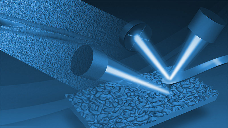
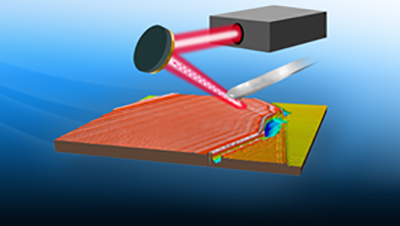
Compared to s-SNOM, photothermal AFM-IR is a relatively new technique for the study of 2D materials. Both techniques are shown schematically in Figure 1. In AFM-IR, pulsed, tunable IR light is focused onto the sample at the AFM tip location. When the IR wavelength matches an absorption band of the material, rapid local thermal expansion excites cantilever oscillations, which are measured by the AFM. The photothermal AFM-IR signal is a direct measurement of sample absorption, and resulting spectra correlate well with conventional Fourier‑transform infrared (FTIR) spectra in transmission mode.
Early AFM-IR studies (pre ~2015) of 2D materials were limited by relatively weak signals due to the typically small thickness and low thermal expansion coefficient of 2D materials. Subsequent gains in detection sensitivity (down to monolayers/single molecules) and spatial resolution (<5 nm) now make AFM-IR a powerful nanoscale characterization tool for 2D materials. Relative to s-SNOM, AFM-IR provides faster measurements, more straightforward interpretation, and displacement-based detection rather than referenced optical detection, positioning it to accelerate 2D materials research.

Previous Studies of 2D Materials with AFM‑IR
AFM‑IR as a complement to s‑SNOM
AFM‑IR has frequently been applied as a complement to s-SNOM for the study of 2D materials, including plasmon polariton in graphene monolayer2, phonon polariton in hBN3,4 and MoO3 5, and circular dichroism in 2D planar‑chiral metamaterials6. For graphene monolayers, IR images recorded at 930 cm‑1 using both Tapping AFM-IR and s-SNOM showed SPP interference fringes with maximum intensity at the edges of the graphene wedge. Fringe spacing and intensity agree between the two methods, confirming that Tapping AFM-IR probes the same SPP mode.2 In hBN, phonon polaritons have been observed and analyzed in flakes as thin as 4 nm.4
AFM‑IR for unique property characterization
AFM-IR has also accessed properties that are more challenging for purely optical near-field techniques, including heat dissipation mechanisms in graphene, non-radiative states in hBN, photothermal effects in thicker hBN, functionalized graphene, and MXene/graphene oxide hybrids:
- For graphene monolayers, AFM‑IR spectra from a graphene flake and SiO2 substrate show strong hybridization between graphene plasmon and SiO2 phonon modes in the 900–1200 cm‑1 range, consistent with the photothermal expansion signal.2
- For hBN frustums (256 nm thick) of varying aspect ratios, AFM-IR spectra showed a broad range of peaks, including some strong ones above 1550 cm‑1 that were assigned to non‑radiative higher order modes, with a wide range of angular and radial momenta.3
- AFM-IR has further revealed large photothermal expansion in nanostructured hBN governed by height-to-width aspect ratio, an effect attributed to the large anisotropy of the thermal expansion coefficients of hBN as well as the nanostructuring implemented.7
- There have been many studies on functionalized graphene materials.8‑11 In one such study, three different functional groups were covalently attached to the graphene basal plane in a dense and well‑defined pattern. The AFM‑IR results, shown in Figure 2, clearly demonstrated the contrast between patterned regions and the underlying graphene layer, as well as the distinctions among the different functionalized patterns.10
- AFM‑IR has also been employed to study hydrogen bonds formed between MXene and graphene oxide nanosheets, which were found to increase the stability of the nanocomposites by reducing the overall energy of the system.12

Case Studies
AFM‑IR study of phonon polaritons in hBN
SPPs and phonon polaritons (PhPs) in 2D materials have high spatial confinement, presenting new opportunities for enhanced light–matter interaction, super lenses, subwavelength metamaterials, and other novel photonic devices. Compared to graphene’s SPPs, hBN’s PhPs exhibit lower loss, especially in isotopically enriched or suspended hBN, enabling longer polariton lifetimes and propagation lengths.
Tapping AFM-IR measurements for a thin hBN flake on a Si/SiO2 substrate over the upper Reststrahlen band (1360–1600 cm‑¹) show a clear correlation between the phonon polaritons and the exciting wavelengths. Results are consistent with theory and prior s‑SNOM observations13, thereby validating AFM-IR for quantitative phonon polariton studies.
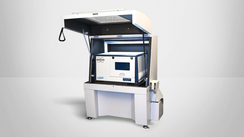
Figure 3 shows the topography and Tapping IR images of a flat, 75 nm thick hBN flake on Si/SiO2, measured on a Dimension IconIR® system. A sequence of Tapping IR images were collected from 1400 to 1580 cm‑1 in 20 cm‑1 steps, with three representative images at 1480, 1520, and 1560 cm‑1 shown. For all three IR images, fringe patterns due to the interference of surface polariton waves were clearly observed.


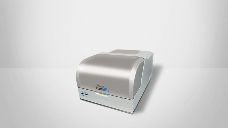
By analyzing the fringe patterns in each Tapping AFM‑IR image, the polariton wavelength, λp, can be easily calculated by doubling the fringe period. The fringe period was averaged across multiple fringes over several pixels to get a value with high accuracy. Then the corresponding momentum, q, can be calculated as q = 2ϖ/λp. The calculated results for all the excitation wavelengths are shown in Figure 4a. A general trend is that the moment of the polariton waves increases with the energy of the excitation wavelength. Results acquired on a nanoIR3™ instrument are also shown, and are consistent with IconIR data.
Using the theoretical models described by Equation 1 in Reference 13 and the parameters for h10BN in Table S4 of Reference 14, the predicted momentum of hBN polaritons can be calculated as a function of excitation wavelengths in the upper Reststrahlen band. The theoretical results are represented by the dashed curve, and the general trend agrees with the experimental data.
Furthermore, an array of 210 spectra were collected with Tapping AFM‑IR across the hBN/SiO2 boundary and into the hBN flake, at a spacing of 12.5 nm and with the array perpendicular to the hBN edge. The IR signal intensity of the normalized spectra is plotted as a function of distance from the hBN/SiO2 boundary in Figure 4b. The resulting spatio‑spectral image shows the polaritonic features in the same pattern as observed in s‑SNOM imaging13, confirming AFM‑IR as an effective technique for studying phonon polaritons in hBN.
AFM‑IR study of stacking order in multilayer graphene
Multilayer graphene can adopt different stacking orders, such as Bernal (ABAB), rhombohedral (ABCA or ACBA), or intermediate (ABCB). Stacking order has a strong influence on the material’s electronic properties; therefore, it is critical to identify stacking order for the purposes of device fabrication. Identification poses a challenge, however, for conventional techniques (e.g., angle‑resolved photoemission, infrared spectroscopy, and Raman spectroscopy) that either lack sufficient resolution or provide only relative contrast, making it difficult to unambiguously identify stacking orders in multilayer graphene. In collaboration with the group of Prof. Andrea Young (Department of Physics, UC Santa Barbara), we applied photothermal AFM‑IR together with scanning microwave impedance microscopy (sMIM) to address this limitation.15
Tapping IR imaging provided robust contrast between domains in a trilayer and tetralayer graphene sample (Figure 5). Domains with different stacking orders were identified through cross‑validation of AFM‑IR, sMIM, and coherent Raman. These domains result in different electrical properties, which were confirmed by sMIM. AFM‑IR spectra acquired at three different domains further revealed clear differentiation in specific IR spectral fingerprints, such as the characteristic resonance at 1576 cm‑1.


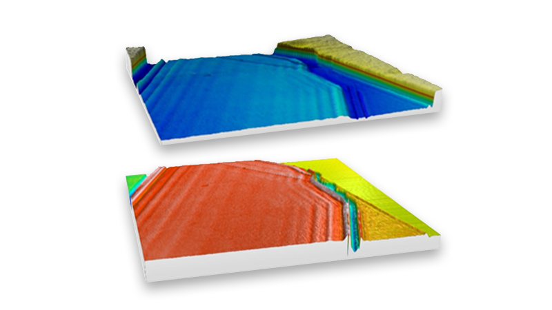
High‑resolution AFM‑IR imaging also revealed narrow domain walls separating different regions of multilayer graphene. The domain walls are associated with shear strain involved in transitions between domains across the graphene flake. Figure 6 shows the topography and IR absorption images at 1576, 1260, and 1128 cm‑1, with several stacking orders identified. Furthermore, a domain wall separating two rhombohedral (ABCA and ACBA) regions was clearly visible in IR images at 1260 and 1128 cm‑1, and a detailed analysis revealed the width of the domain wall at the 10 nm scale.
AFM‑IR is also well suited to image graphene layers incorporated into van der Waals heterostructures. Figure 7 shows the topography and IR image of trilayer flakes containing both rhombohedral (ABC) and Bernal (ABA) stacked regions, covered by 5−10 nm of hBN. Some bright dots were observed in the topography image due to air bubbles trapped between the graphene trilayer and outer hBN layer; otherwise, the graphene flakes exhibit a smooth profile. The IR images show more detail: at 1576 cm‑1 there is higher signal for the ABC trilayer than the ABA trilayer, similar to the contrast for uncapsulated graphene trilayer in Figure 5. Inverse contrast was observed between the ABC and ABA trilayers in the IR image at 1128 cm‑1.
These results demonstrate that AFM‑IR, combined with correlative techniques (such as sMIM in this study), is effective in studying graphene stacking orders, as well as detecting nanoscale walls between different domains and imaging buried graphene layers within van der Waals heterostructures.

AFM-IR Correlates Structure and Chemistry in 2D Materials at the Nanoscale
Photothermal AFM-IR has proven to be a powerful technique for studies on 2D materials, including those on plasmon polaritons in graphene and phonon polaritons in hBN, as presented here. AFM‑IR produces results that are complementary to s‑SNOM, while also introducing unique capabilities. Unlike s‑SNOM, AFM‑IR can easily provide data on non-radiative “dark” states, heat transfer mechanisms, and the chemistry of functionalized graphene. With its superior detection sensitivity, spatial resolution, measurement speed, and ease of use, AFM‑IR will meet the growing need for a deeper understanding of 2D materials and support the search for new materials.
Authors
- Qichi Hu, Ph.D., Sr Staff Applications Scientist (qichi.hu@bruker.com)
- Cassandra Phillips, Ph.D., Sr Product Manager Nanoscale IR Spectroscopy (cassandra.phillips@bruker.com)
- Hartmut Stadler, Ph.D., Application Scientist (Hartmut.Stadler@bruker.com)
- Alireza Fali, Ph.D., Sr Development Engineer (alireza.fali@bruker.com)
- Jinhee Kim, Ph.D., Applications Scientist (jin_hee.kim@bruker.com)
- Peter De Wolf, Ph.D., Sr Director of Technology and Application Development (peter.dewolf@bruker.com)
References
- Pham, P.v., Bodepudi, S.C., Shehzad, K., et al. 2022. “2D Heterostructures for Ubiquitous Electronics and Optoelectronics: Principles, Opportunities, and Challenges.” Chemical Reviews 122 (6): 6514–613. DOI: 10.1021/acs.chemrev.1c00735
- Menges, F., Yang, H., Berweger, S., et al. 2021. “Substrate-Enhanced Photothermal Nano-Imaging of Surface Polaritons in Monolayer Graphene.” APL Photonics 6 (4). DOI: 10.1063/5.0044738
- Brown, L.v., Davanco, M., Sun, Z. et al. 2018. “Nanoscale Mapping and Spectroscopy of Nonradiative Hyperbolic Modes in Hexagonal Boron Nitride Nanostructures.” Nano Letters 18 (3): 1628–36. DOI: 10.1021/acs.nanolett.7b04476
- Ciano, C., Giliberti, V., Ortolani, M., and Baldassarre, L. 2018. “Observation of Phonon-Polaritons in Thin Flakes of Hexagonal Boron Nitride on Gold.” Applied Physics Letters 112 (15). DOI: 10.1063/1.5024518
- Schwartz, J.J., Krylyuk, S. Jakob, D.S., et al. 2023. “Mid-Infrared, Near-Infrared, and Visible Nanospectroscopy of Hydrogen-Intercalated MoO3.” The Journal of Physical Chemistry C 127 (34): 17002–13. DOI: 10.1021/acs.jpcc.3c05114
- Khanikaev, A.B., Arju, N., Fan, Z., et al. 2016. “Experimental Demonstration of the Microscopic Origin of Circular Dichroism in Two-Dimensional Metamaterials.” Nature Communications 7 (1): 12045. DOI: 10.1038/ncomms12045
- López, J.J., Ambrosio, A., Dai, S., et al. 2018. “Large Photothermal Effect in Sub-40 Nm h-BN Nanostructures Patterned Via High-Resolution Ion Beam.” Small 14 (22). DOI: 10.1002/smll.201800072
- Bartlam, C., Morsch, S., Heard, K.W.J., et al. 2018. “Nanoscale Infrared Identification and Mapping of Chemical Functional Groups on Graphene.” Carbon 139 (November): 317–24. DOI: 10.1016/j.carbo.2018.06.061
- Liu, Z., Nørgaard, K., Overgaard, M.H., et al. 2018. “Direct Observation of Oxygen Configuration on Individual Graphene Oxide Sheets.” Carbon 127 (February): 141–48. DOI: 10.1016/j.carbon.2017.10.100
- Rodríguez González, M.C, Leonhardt, A., Stadler, H., et al. 2021. “Multicomponent Covalent Chemical Patterning of Graphene.” ACS Nano 15 (6): 10618–27. DOI: 10.1021/acsnano.1c03373
- Kumagai, R., Takahashi, M., Suzuki, N., et al. 2025. “Nanoscale Chemical Characterization of Functionalized Graphene by Heterodyne AFM-IR and Chemical Force Microscopy.” Nanoscale 17 (29): 17016–23. DOI: 10.1039/D5NR01862E
- Yang, J., Li, M., Fang, S., et al. 2024. “Water-Induced Strong Isotropic MXene-Bridged Graphene Sheets for Electrochemical Energy Storage.” Science 383 (6684): 771–77. DOI: 10.1126/science.adj3549
- Dai, S., Fei, Z., Ma, Q., et al. 2014. “Tunable Phonon Polaritons in Atomically Thin van Der Waals Crystals of Boron Nitride.” Science 343 (6175): 1125–29. DOI: 10.1126/science.1246833
- Giles, A.J., Dai, S., Vurgaftman, I., et al. 2018. “Ultralow-Loss Polaritons in Isotopically Pure Boron Nitride.” Nature Materials 17 (2): 134–39. DOI: 10.1038/nmat5047
- Holleis, L., Cohen, L., Samuelson, N., et al. 2025. “Nanoscale Infrared and Microwave Imaging of Stacking Faults in Multilayer Graphene.” Nano Letters 25 (33): 12487–94. DOI: 10.1021/acs.nanolett.5c02301
©2026 Bruker Corporation. All rights reserved. Dimension IconIR and nanoIR3 are trademarks of Bruker Corporation. All other trademarks are the property of their respective companies. AN210, Rev. A0.