
XFlash oval: A Windowless, High Collection Angle EDS Detector for Enhanced Analysis
A Unique EDS Detector for Ultra-High Resolution Elemental Mapping
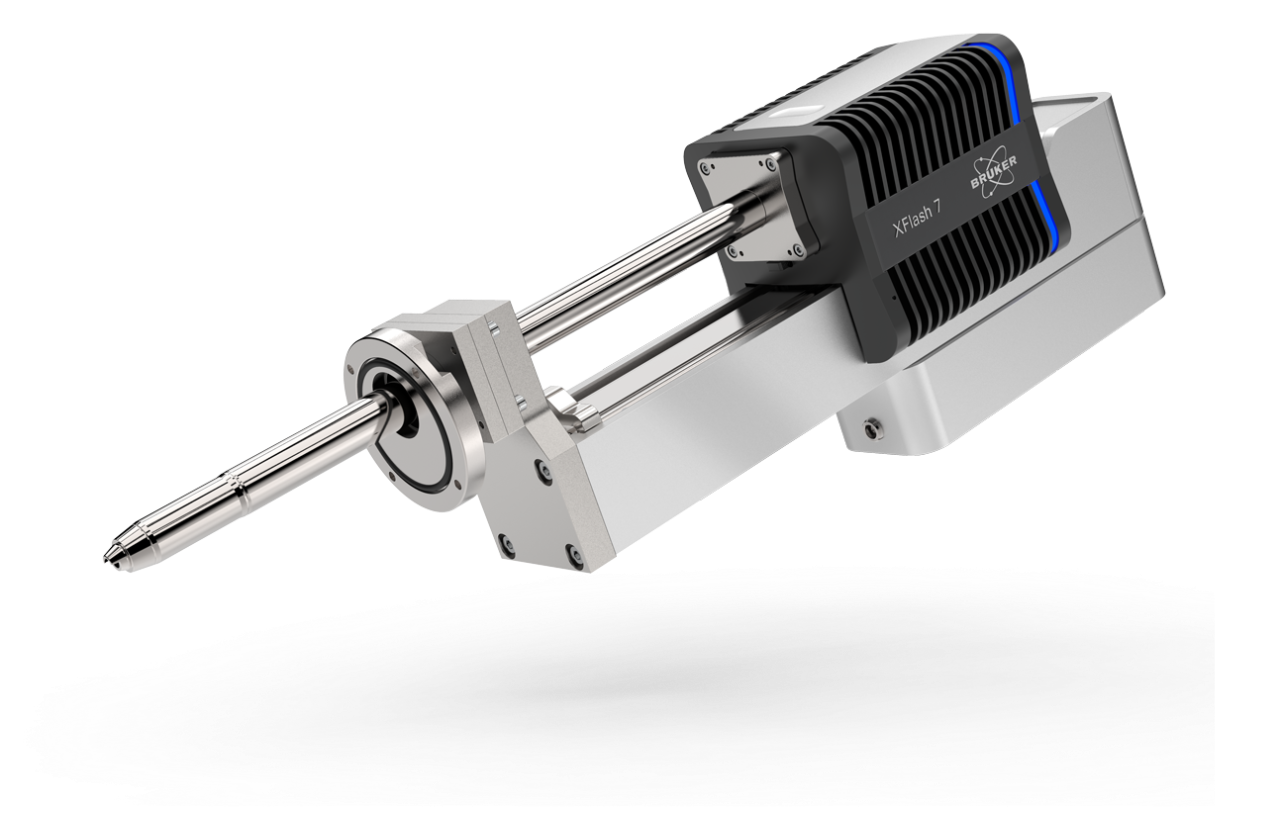
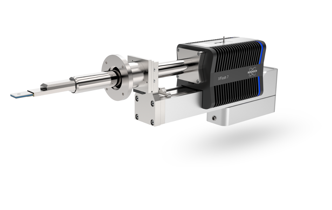
We announce the release of a new large collection angle EDS detector with an oval shaped SDD area of 100 mm2, the XFlash® T oval for TEM and STEM and the XFlash® oval for SEM and T-SEM.
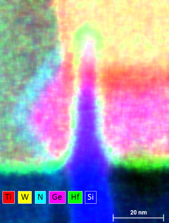
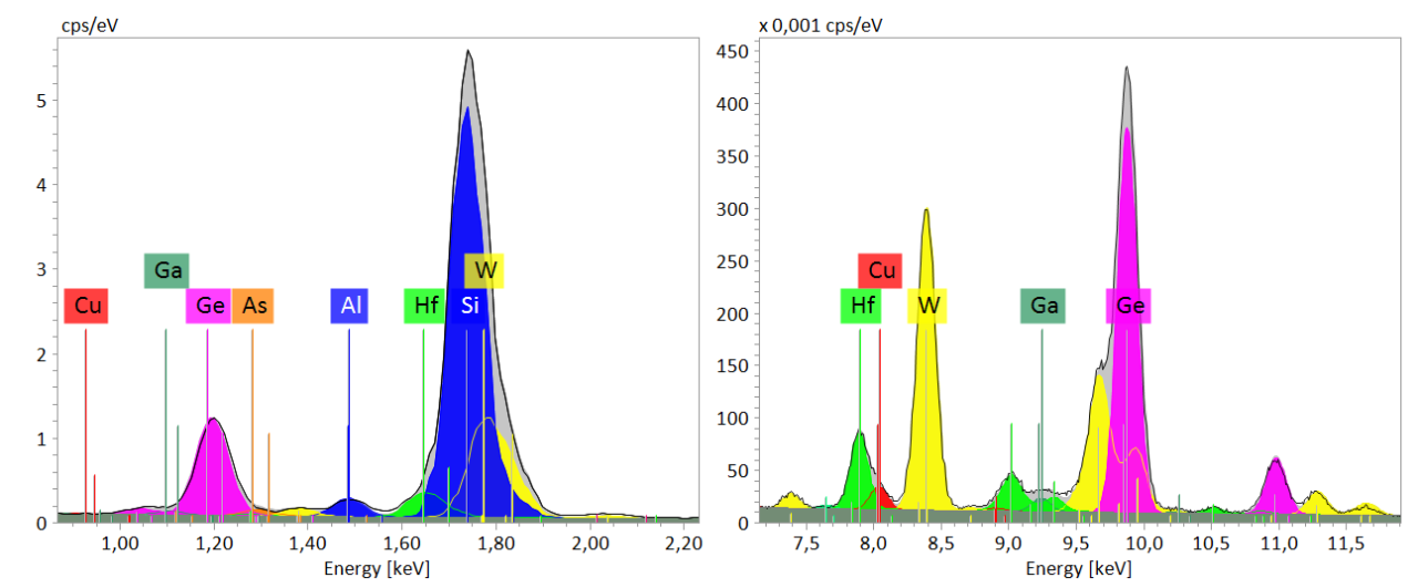
This webinar will inform about the detector features, specifics of microscope detector geometries as well as respective data acquisition and analysis. Qualitative and quantitative element mapping for different large collection angle EDS settings will be explained (Fig. 1, 2) and related to results obtained by standard EDS.
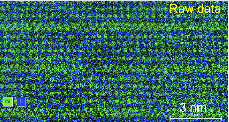
The detector has been shown to provide collection angles between 0.4 sr to 0.7 sr at high take-off angles of around 12° on TEM/STEM and collection angles of up to 0.4 sr on SEM. The pole piece to detector geometry is optimized for each specific microscope type in cooperation with the microscope manufacturer. This enables fast and routine element mapping at the nanometer scale without compromising the microscope performance, suitable electron probe quality and specimen preparation provided. In STEM atom column EDS (Fig. 3, [1]) as well as single atom identification [2] become possible.
[1] Direct atomic scale determination of magnetic ion partition in a room temperature multiferroic material L. Keeney et al., Scientific Reports 7, Article number: 1737 (2017), open access
[2] Individual heteroatom identification with X-ray spectroscopy R. M. Stroud et al., APL 108, 163101 (2016), open access
Watch more XFlash
Who should attend?
- Scientists and application scientists from industry and academia working in microscopy and the characterization of inorganic and organic materials
- Interested in efficient fast high spatial resolution high-end EDS in TEM and STEM
- Interested in standard EDS of electron transparent specimens
Speakers

Dr. Meiken Falke
Global Product Manager EDS/TEM, Bruker Nano Analytics
Andi Kaeppel
Senior Product Manager EDS / SEM, Bruker Nano Analytics
Watch this Webinar On-Demand
Please enter your details below to gain on-demand access to this webinar.