Solving Challenges in Defect Inspection of Advanced Optics
Optical components such as lenses, mirrors, prisms, and windows undergo tight quality control to deliver optimal optical transfer function.
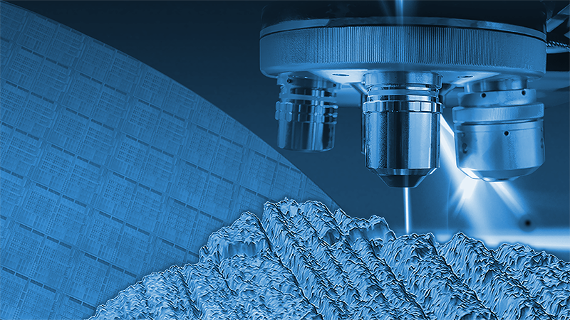
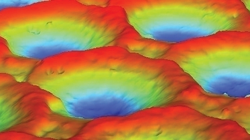
This webinar focuses on how WLI-based 3D optical profilers uniquely combine subnanometer vertical resolution over mm2 large areas to enable 100% inspection of high-quality optics through direct measurement of topography.
Viewers can expect to gain new insight into the imperfection inspection process for advanced optical materials, including the ideal strategies for defect detection, ranking, and mapping for complex geographies and large and aspheric optics.
Webinar Summary
Lenses, mirrors, prisms, windows and other optical components are subject to strict quality control standards. These are essential to ensuring the optimal transfer function of advanced optical materials; any scratch, dig, chip pinhole, or other defect will trigger wide-angle scattering of a light beam, reducing the quality of the end product.
Well-defined quality control tests--such as the military standard, MIL-PRF-13830B--are used to assess the number, type, and density of defects, as well as the percentage of defective areas. These inspections rely on direct or indirect optical methods to reveal defects and rank them. However, these techniques are, at best, contour detection-based--often with tedious manual operation or need for operator judgment--and fail to report accurate roughness measurements or deliver information required for advanced optics used in gyrolaser navigation systems, high-power laser beams, extreme UV lithography tools, etc.
Geared toward engineers, researchers, QA and QC professionals, optical designers, and executives and managers concerned with inspecting and preventing defects in advanced optical components (including those used in semiconductors and microelectronics, additive manufacturing, automotive, and aerospace applications), this webinar explains how customized analysis enables optical profiler users to:
- Easily spot minute defects, even for complex surface geometries;
- Automatically generate critical information of detected defects (size, depth/height, orientation, location) without operator intervention or an etching step;
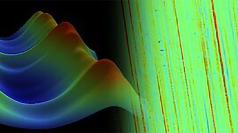
- Accurately characterization of roughness along mid- and short-spatial wavelengths, complying to ISO norm 10110-7/8; and
- Better understand the root causes for defects and allows further optimization in the polishing process to meet more stringent specifications.
This webinar was presented on September 23, 2019.
Find out more about the technology featured in this webinar or our other solutions for defect inspection of optical components: