XFlash 6-60
The Large Area SDD for Nano-Analysis
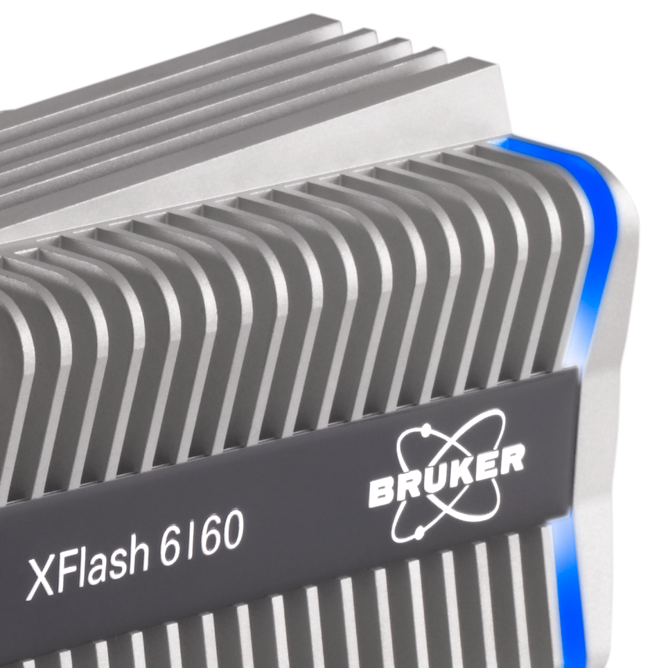
The XFlash 6-60 detector
The large active area 60 mm2 chip together with the slim-line detector finger provide a large solid angle. The XFlash® 6-60 is therefore predestined for use in applications with relatively low X-ray yield, as common in the area of nano-analysis. As the detector also delivers a very good energy resolution with 126 eV at Mn Kα and the according C and F resolutions, it can also comfortably be used in the low energy range, which is also an requirement in this field.
In summary, the XFlash® 6-60 offers the following advantages:
- Very good energy resolution (126 eV at Mn Kα, 51 eV at C Kα and 60 eV at F Kα available)
- Other available resolution is 129 eV at Mn Kα
- Extremely high pulse load capability
- Excellent light element and low energy performance (element range Be - Am)
- No elaborate, vibration-generating cooling systems
- Immediately available after power on
- Low operating cost
- Maintenance-free operation
- Small dimensions, including slim-line technology finger
- Low weight
Suggested areas of application for the XFlash® 6-60 are:
- EDS systems for SEM, microprobe, FIB-SEM (welded bellows available as an option)
- Combined EDS and high resolution EBSD analysis with the eFlash FS
- Nano-analysis