Nanolithography
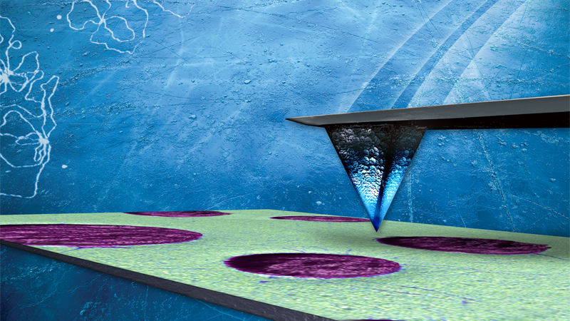
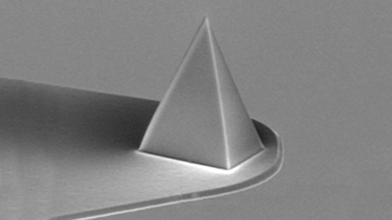
Some of the most progressive studies in nanotechnology require the precise fabrication and interconnection of nanometer-scale structures. Anodic oxidation nanolithography uses an applied voltage to the AFM probe to create an oxide layer directly under the tip. Since the oxide only forms under the tip, very narrow oxide lines can be written on the sample.
Bruker’s NanoMan and NanoPlot software packages provide a user-friendly interface for high-definition nanolithography with a variety of "writing" techniques, in either a graphical point-and-click mode, or in a recipe-driven mode. Lithography is also possible on the Dimension Icon® system using Piezoresponse Force Microscopy (PFM).


Your download is now available.
Note: If you exit this page, you may not be able to reopen this download window without re-submitting the form.
