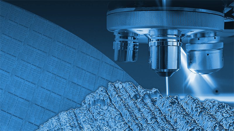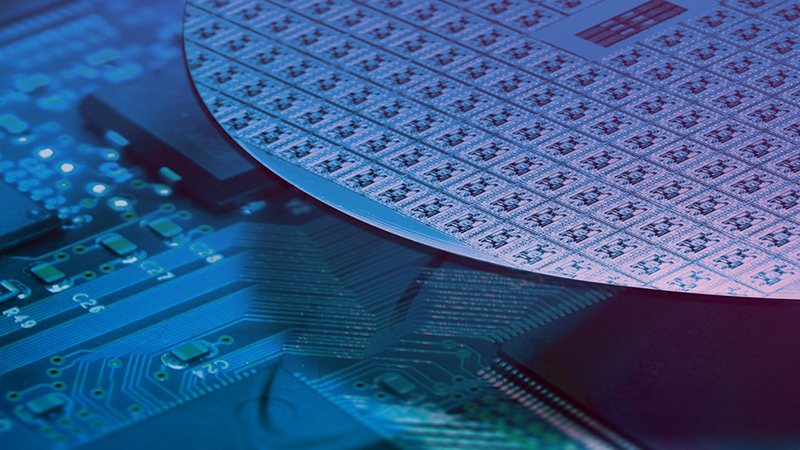
Accelerating Semiconductor Processes Control with Advanced 3D Optical Metrology
Increastingly strict tolerances make fast, precise front- and back-end process control a critical part of semconductor device and component production.
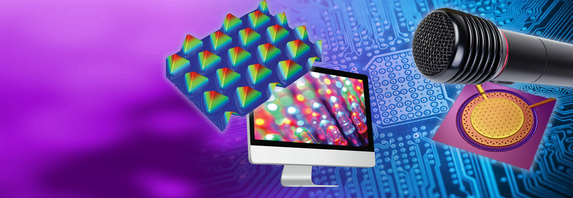
This webinar presents case studies demonstrating the use of 3D optical profilers for improving yield, identifying root cause failure, and driving next-generation device development from bare wafer to final packaged device.
Viewers can expect to gain new insight into bare wafer roughness control and CMP monitoring and optimization as well as the use of direct measurement of topography to assess die flatness and identify the source of RDL, bump, recess, and overlay defects.
Webinar Summary
Explore Advanced Process Control Techniques for Semiconductor Manufacturing
Designed for Process, CMP, and Metrology & Quality Engineers as well as R&D scientists working in semiconductor, micro-electronics, display technology, printed electronics, and telecoms industries, we cover requirements and metrology needs for:
- Advanced telecommunication
- Compact on-board electronics
- Electric vehicles
- Denser interconnect networks
- Finer redistribution layer (RDL)
- Direct wafer to wafer bonding
- Wafer fan-out packaging
Among the included case studies, front end (FEOL) examples will include:
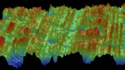
- Wafer bin roughness and edge roll-off
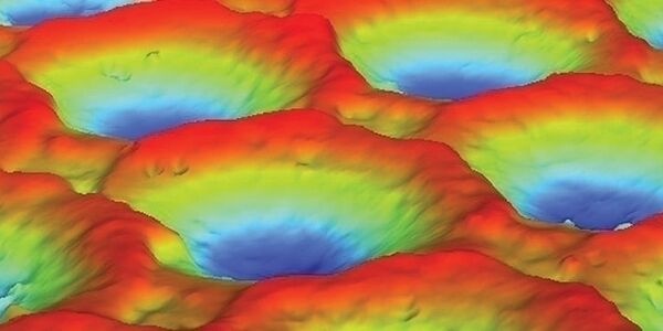
- CMP efficiency full die flatness
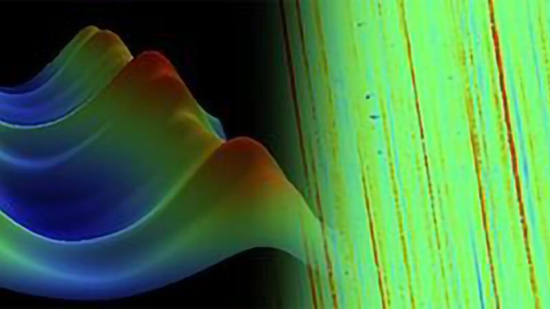
- CD metrology including TSV, deep trench RIE (Bosch process)
- Epi layer defect quantification in high power devices
Back end (BEOL) and packaging examples will address:
- Under Bump Metallization (UBM)
- Recess defect inspection
- Full die screening for dense interconnect control
This webinar was presented on December 17, 2018.
Find out more about the technology featured in this webinar or our other solutions for semiconductor process control: