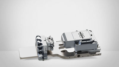
TKD and STEM Compatible Hysitron PI 89
The Hysitron PI 89 is now available for analytical imaging of electron transparent samples using TKD and STEM detectors while performing nanomechanical testing. The Transmission Kikuchi Diffraction technique (TKD), has been recently introduced for Scanning Electron Microscopes (SEM) to provide 10x better spatial resolution of a sample compared to the established Electron Backscatter Diffraction (EBSD) technique. By utilizing quickly attached components, the Hysitron PI 89 system can be modified to create the additional needed space to insert a detector under the sample, thus obtaining the best possible signal. Bruker’s patented PTP device can be used for tensile testing in TKD mode to provide superior stability to the sample.
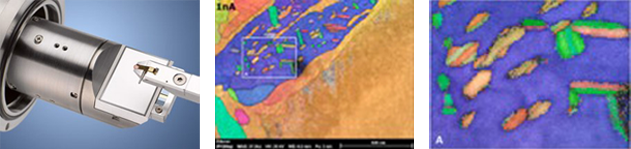
The unique design of Bruker’s OPTIMUS TKD detector allows user to place the detector directly underneath the sample. Alongside the e-Flash EBSD detectors, the OPTIMUS can obtain the strongest signal with the least gnomonic projection induced distortions.