Crystalline Defect Inspection
Crystalline Defect Inspection
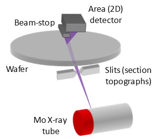
X-ray diffraction imaging (XRDI, also known as X-ray topography) and micro-XRF are used to image crystalline defects in otherwise perfect (or near perfect) substrates. In Si manufacturing the main application is for the screening of cracks and defects at the edge of the wafer which may cause wafer breakage further downstream. This is non-destructive, non-contacting method which measures product wafers with no sample preparation needed.
X-ray Diffraction Imaging
Defects Characterized
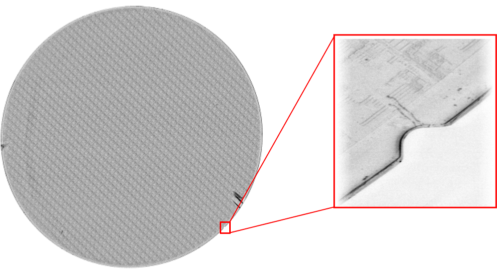
Product wafers are measured at high throughput with resolution sufficient for the damaging defects. The images are automatically analyzed and the defects detected and characterized. By utilizing the comprehensive information about the defect, it is possible to determine whether a wafer has a higher probability of breakage, optimize wafer flow and identify the likely process equipment upstream which has created the defect.
Non-Destructive Cross Section
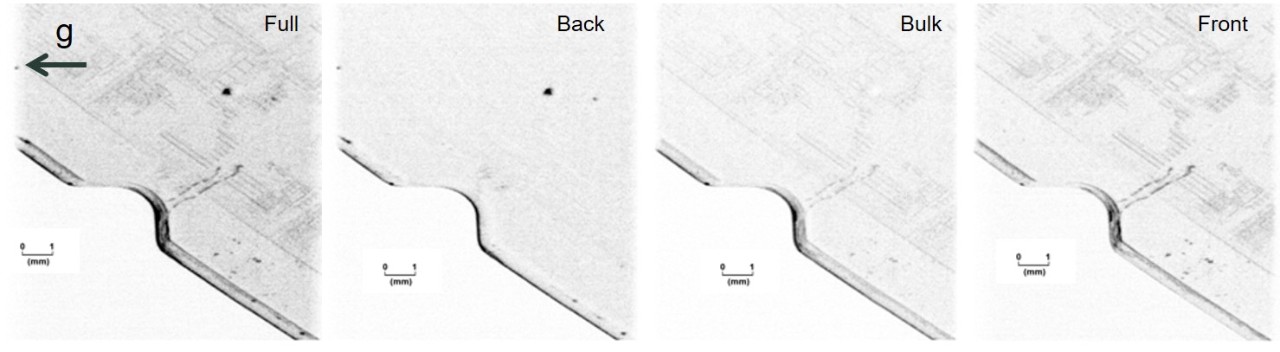
Once a defect is identified it can be optionally measured at a higher resolution to find out more information about the nature, size and exact type of defect. Non-destructive cross sections can indicate whether the defect is on the front or back side, or through the bulk of the wafer.
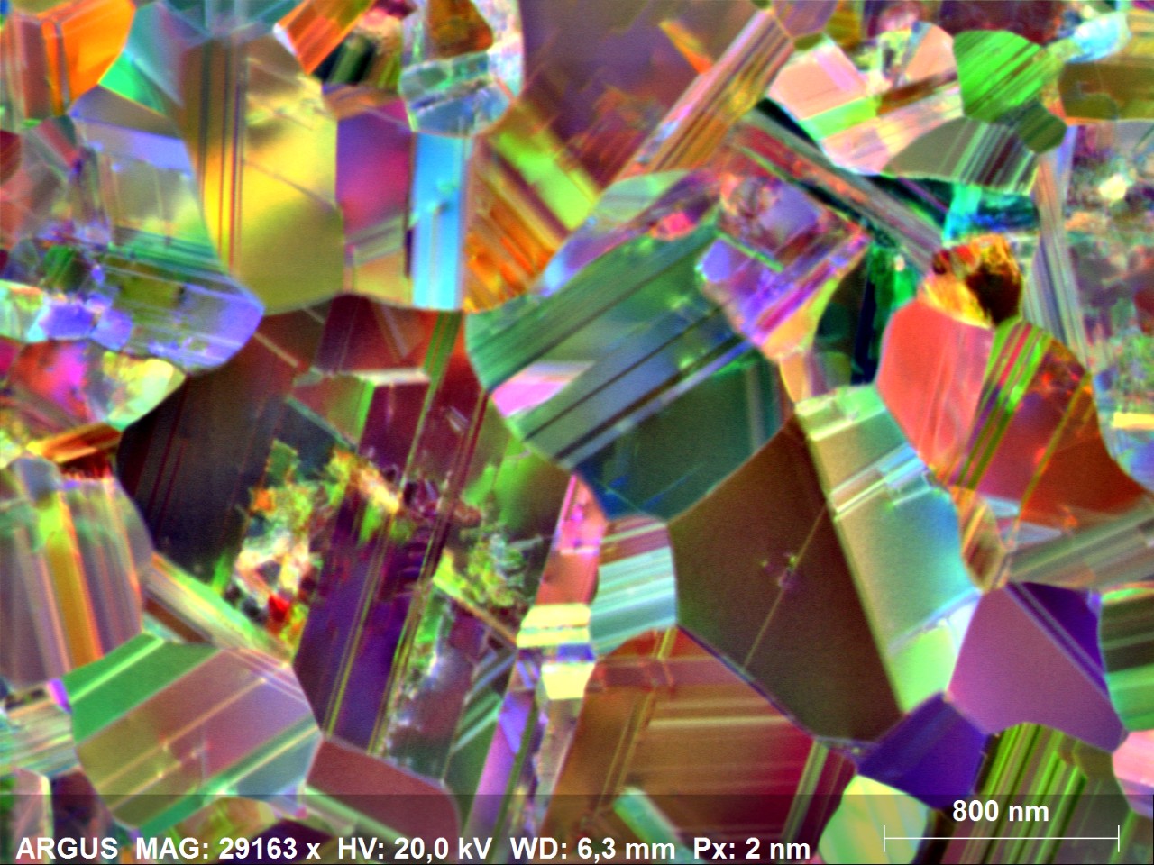
EBSD and TKD
Crystalline defects can be imaged using the most sensitive orientation contrast imaging detector for SEMs, ARGUS. Bruker's state of the art imaging system for EBSD and TKD detectors allows mapping orientation changes below 0,1° at speed of up to 125 000 pps with unmatched high contrast and low noise images.
When a simple and quick visualization of the homogeneity or changes is required, micro-XRF allows visualizing Bragg type artefacts from micro-XRF mappings. This allows a quick inspection with a very versatile analytical tool.
Explore further application examples on our Application notes: