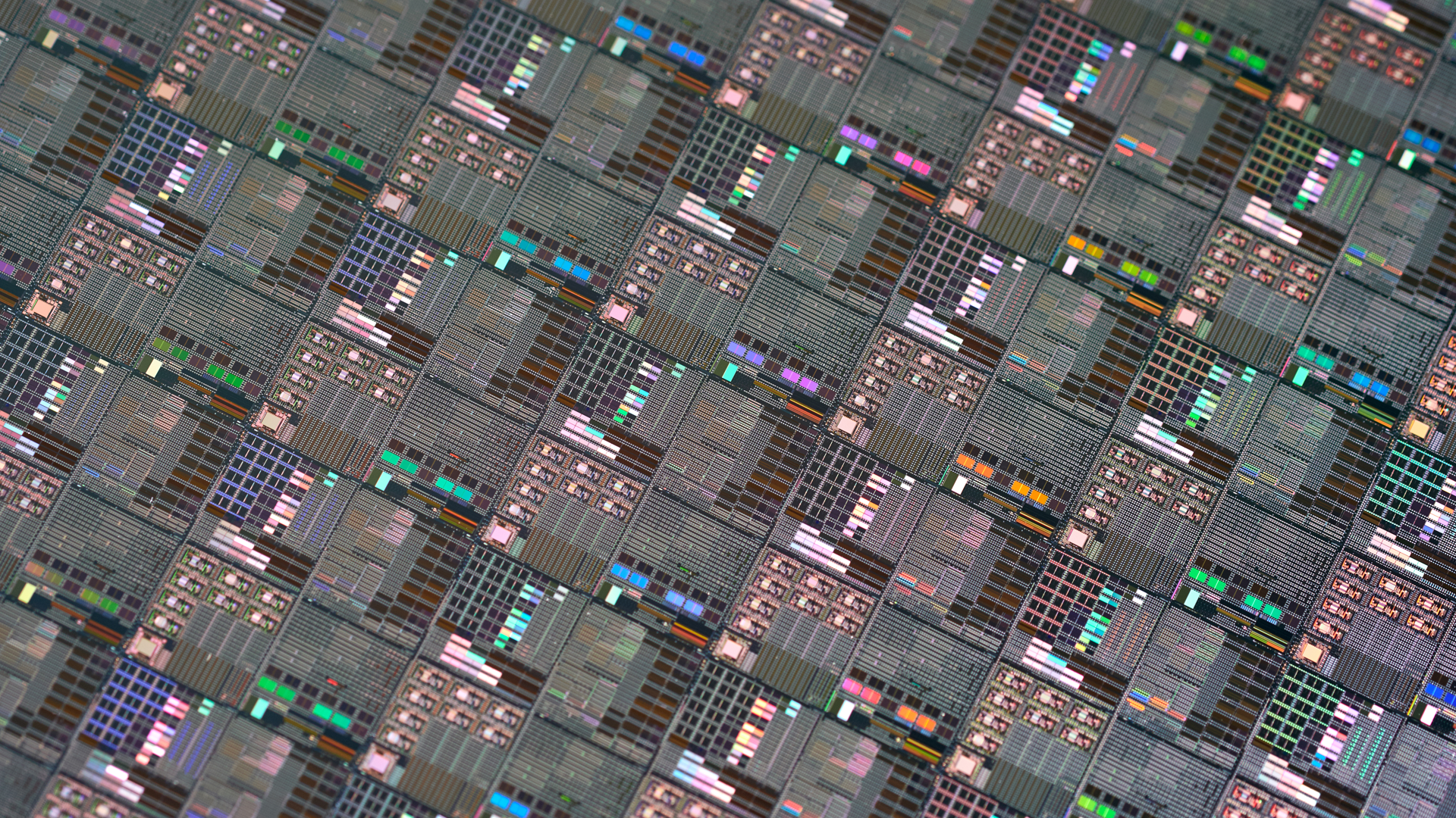
X-Ray Metrology for Compound Semiconductor
X-Ray Metrology for Compound Semiconductor
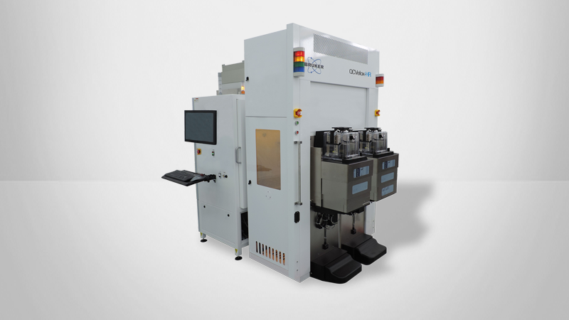
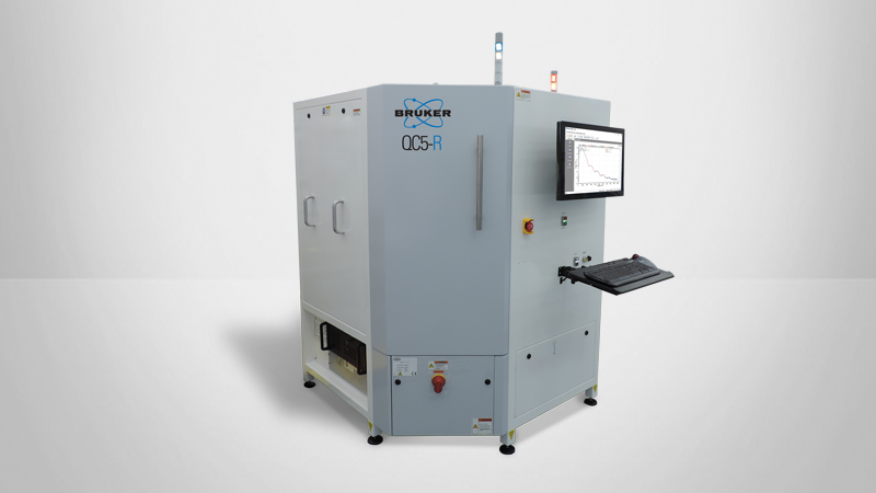
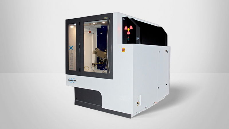
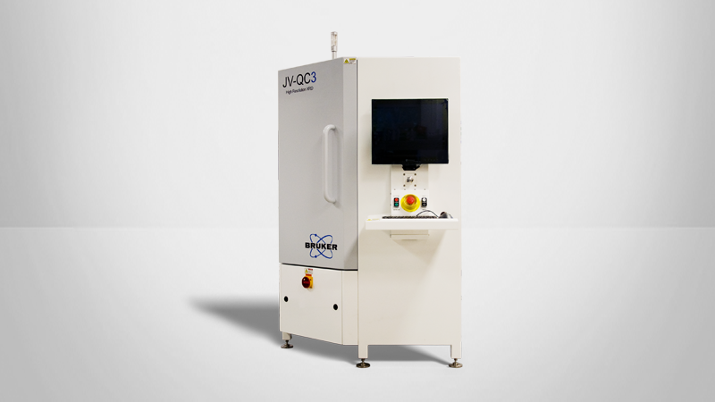
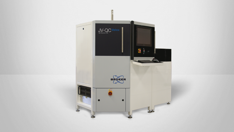
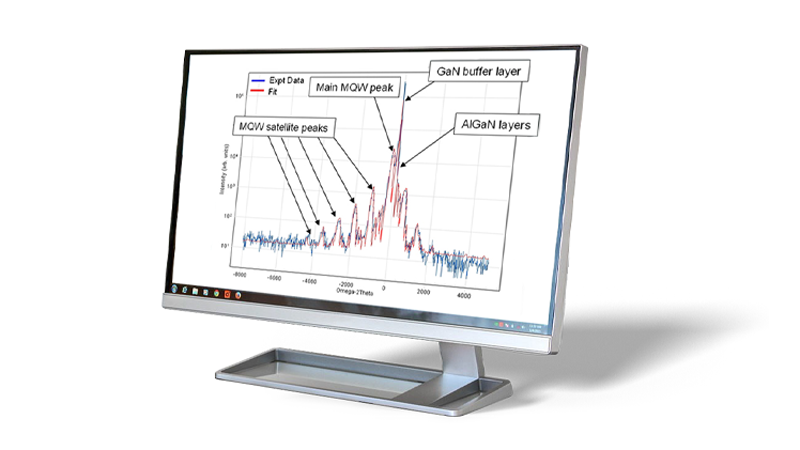
Bruker provides X-ray metrology tools for both QC monitoring of epilayer films and for detailed R&D analysis of a wide range of semiconductor films and wafers. We offer systems designed specifically for the challenging demands of the production environment, as well as multi-application research tools for development supporting current and future metrology needs.
Support

How Can We Help?
Bruker partners with our customers to solve real-world application issues. We develop next-generation technologies and help customers select the right system and accessories. This partnership continues through training and extended service, long after the tools are sold.
Our highly trained team of support engineers, application scientists and subject-matter experts are wholly dedicated to maximizing your productivity with system service and upgrades, as well as application support and training.