Film Thickness Determination
Chemical Identification of Thin Films and Monolayers by FT-IR
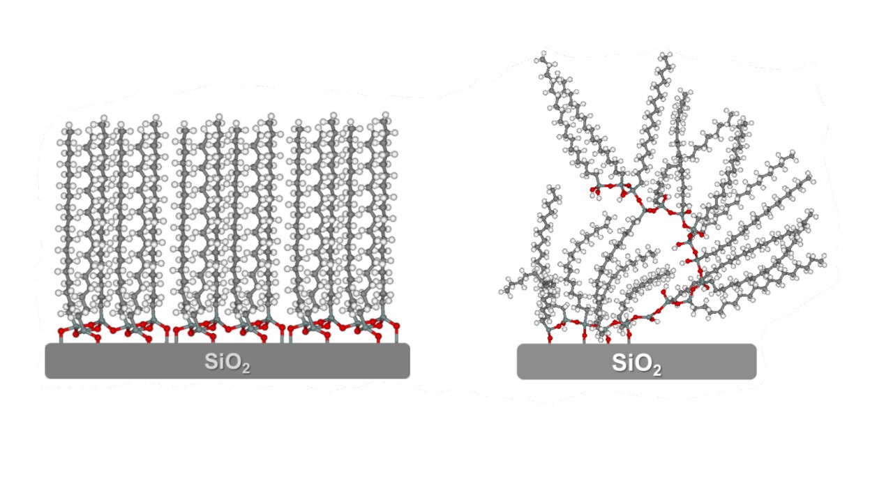
Surface functionalization and modification with ultra-thin films play an important role in many application fields such as biofouling, sensorics, corrosion protection, catalysis etc. This makes the thorough investigation of such films mandatory, to understand and improve the film growth and functionality. There are numerous methods to chemically identify films and coatings using FTIR spectroscopy.
These are transmittance, attenuated total reflection (ATR), gracing angle reflectance (GIR) or infrared reflection absorption spectroscopy (IRRAS), polarization modulated IRRAS (PMIRRAS). Depending on the film thickness, optical property and supporting substrates different measurement mode(s) can be preferentially applied.
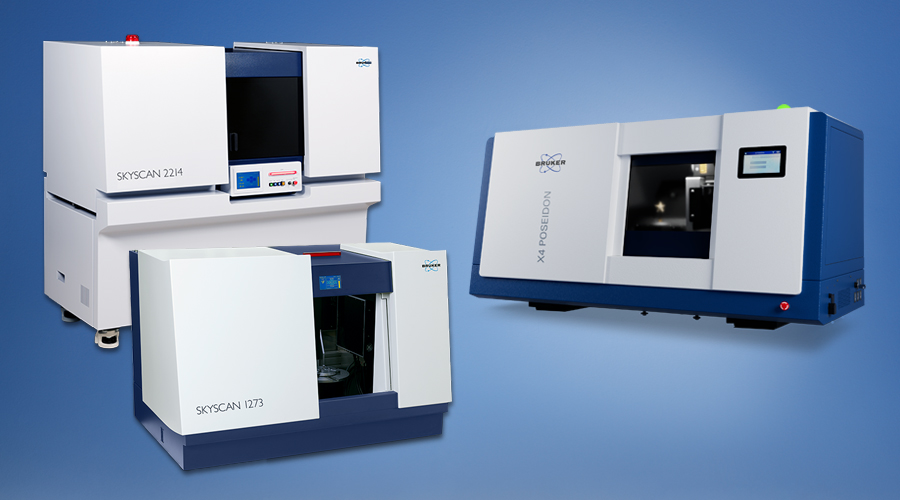
Thin Films Analysis with SEM micro-XRF
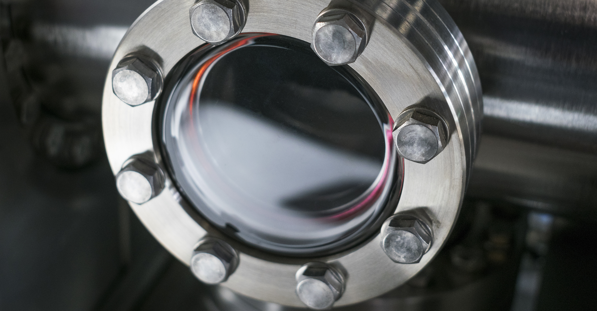
As X-rays may pass through matter, X-ray Fluorescence (XRF) allows the determination of layer thickness. Using micro-XRF on SEM, the layer analysis (thickness and composition) is rendered feasible with spatial resolution at the micrometer scale. Layer analysis is strongly based on quantification using atomic fundamental parameter (FP). It can be improved with the use of standard samples, so various types of layer systems can be investigated by FP, such as metallization on wafer, multi-metal pretreatment coatings and solar cells. Read more
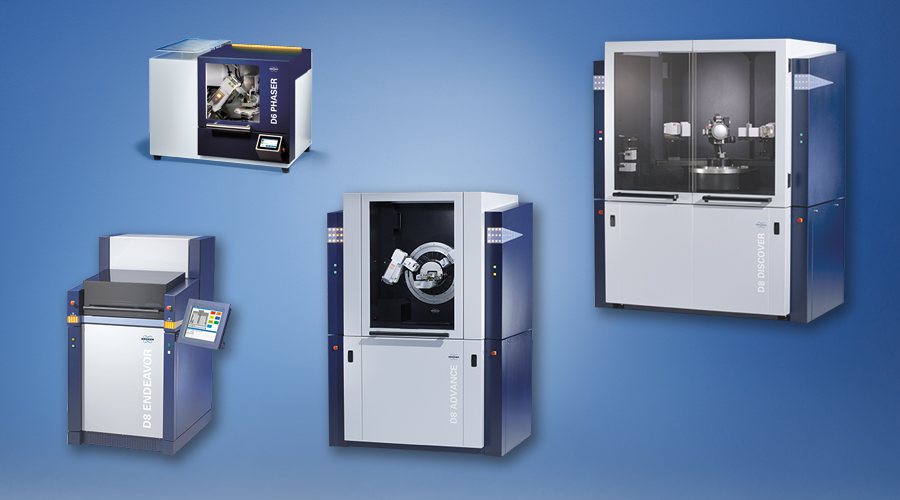
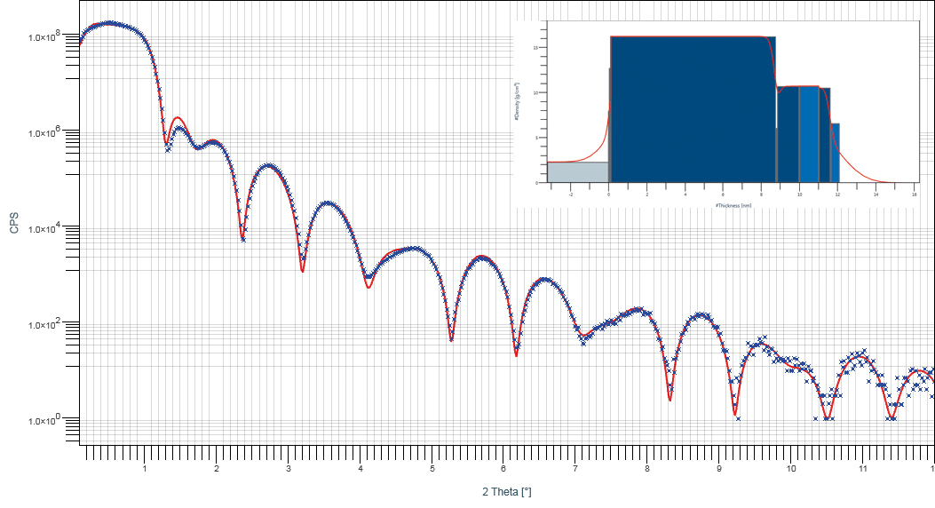
Characterization of a Ta Coating on Si and a GaN/AlN Superlattice with X-ray Reflectometry
All materials exhibit total reflection of X-rays incident below a certain critical angle, giving a reflected intensity nearly as great as the direct beam. As the incident angle is increased when measuring X-ray Reflectometry (XRR), penetration into the material causes the reflected intensity to drop precipitously. XRR data can therefore span many orders of magnitude. XRR is a fast, non-destructive way to measure thickness, roughness and density of thin film coatings, multilayers and superlattices. This information can be extracted from the specular interference pattern and allows characterization of crystalline and amorphous films.
Characterizing GaN Based Materials Using Modern X-ray Methods
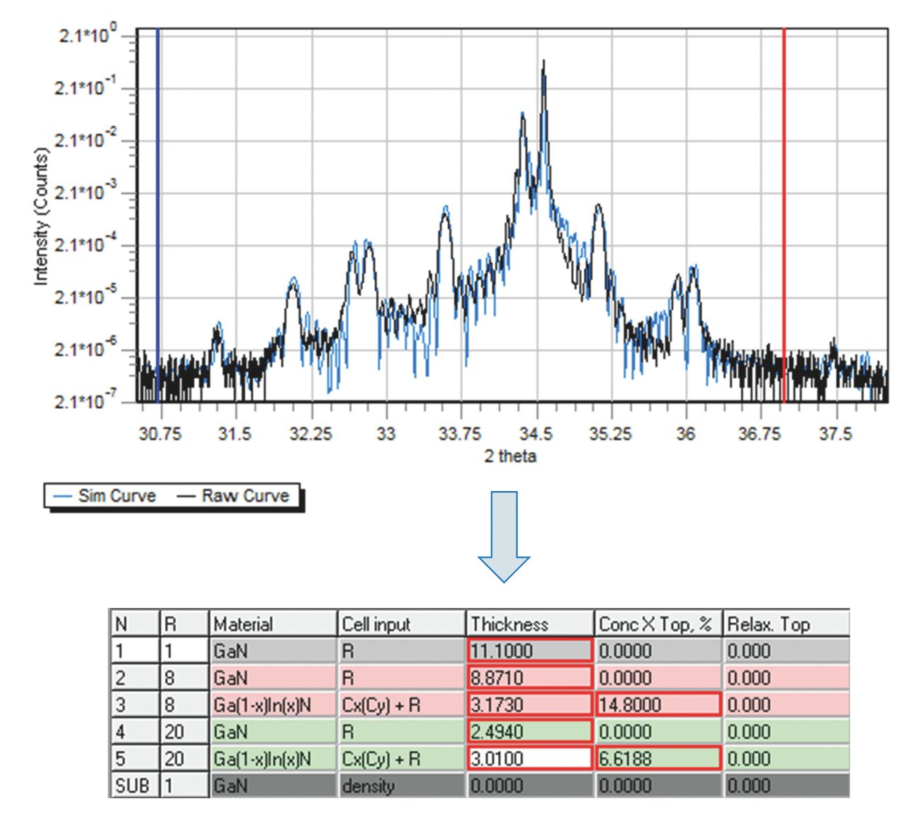
Characterization of Gallium Nitride (GaN) based materials is often done using non-destructive X-ray metrology. A major class of wide band gap semiconductors, GaN and its In/Al equivalent are utilized on substrates of many new devices like high electron mobility transistors (HEMTs), light emitting diodes (LEDs), laser diodes, and solar in the form of thin film epitaxial layers that range from a few nm to microns. Device performance is frequently linked to stacking sequence, layer thickness, crystal structure, and chemical composition. These properties can be studied using High Resolution X-ray Diffraction (HRXRD) with techniques like X-ray Reflectivity (XRR), Reciprocal Space Mapping (RSM), and high-resolution rocking curves (RC).