KO
My Bruker
전문가에게 문의하십시오.
제품 및 솔루션
응용 분야
서비스
뉴스 및 이벤트
소개
채용
최소 두 글자를 사용해 주십시오. (현재 한 글자 사용함)
Languages
Deutsch
English
Español
Français
Italiano
Polski
Português
Русский
中文
日本語
한국어
▶ Watch On-Demand | 55 Minutes
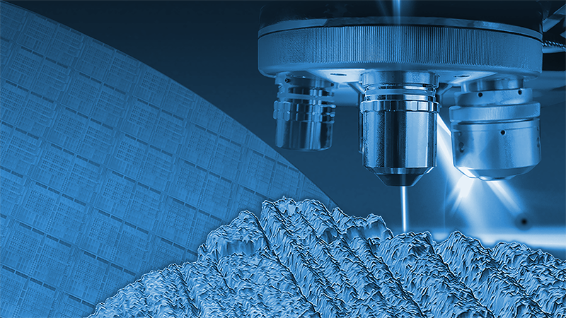
Solving Challenges in Defect Inspection of Advanced Optics
Perform precise, fully automated imperfection and defect inspection of advanced optical components
이 동영상을 재생하려면 쿠키를 허용해야 합니다.
쿠키 설정
Presented by Samuel Lesko, Ph.D., Dir. of Technology and Apps Development, Bruker Nano Surfaces & Metrology (September 23, 2019)
Download Slides
PRESENTATION HIGHLIGHTS:
[00:03:11]
Intro to surface inspection for fine optics for advanced applications
[00:06:28
] Components and modes of non-contact interferometric profilers
[00:14:42]
Quality control of high-end optics
[00:18:45]
Beyond traditional visual inspection
[00:23:30]
Options for 100% automation and full characterization, ranking, monitoring, and mapping of defects
[00:41:18]
For large and aspheric optics
LIVE AUDIENCE Q&A:
[00:45:56]
Can these non-contact methods be used to mesure surface profile as well?
[00:48:24]
Can this method support pass/fail decisions against a scratch-and-dig specification of ISO 10110?
[00:50:42]
What is the visible range for scanning? How long does it take?
[00:52:39]
What are the limitats of this method?
[00:55:46]
Can this method be used to qualify objects in high-volume manufacturing?
Featured Products and Technology
3D Optical Profilers
Non-contact 3D surface measurement, inspection, and analysis
더 읽어보기
REQUEST MORE INFORMATION
3D Surface Measurements
History, advantages, applications, and instrument recommendations
더 읽어보기
REQUEST MORE INFORMATION
Related Webinars
On-Demand Session • 2 Hrs
Surface Finish Optimization for Advanced Manufacturing by Optical Profiler
Learn about the relationship between areal roughness parameters and part/component functionality and how areal roughness measurement drives improvement of surface finishing processes in manufacturing.
On-Demand Session • 1 Hr 5 Minutes
Qualifying Surface and Device Performance Through Roughness Quantification
Learn how to measure micro-roughness in accordance with the ISO 25178 norm to assess device performance and efficiency and, ultimately, improve product and process design.
On-Demand Session • 50 Minutes
Accelerating Semiconductor Processes Control with Advanced 3D Optical Metrology
Discover recent advancements in 3D Optical Metrology and how they accelerate in-line quality control for both front- and back-end processes, supporting next-generation semiconductor device development.
RETURN TO SESSION OVERVIEW