Advances in Piezoresponse Force Microscopy
- Ferroelectric characterization using piezoresponse force microscopy (PFM), with a focus on quantitative measurements and resulting insight in the material properties.
- The role of switching spectroscopy (SS-PFM), contact Kelvin Probe Microscopy (cKPFM), contact resonance-based detection, nano-PUND, and Data Cube approaches in artifact avoidance and maximizing sensitivity on functional materials.
- PFM measurements in highly conducting liquids for life science and energy research.
Watch Recording
Program Notes
Symposium Introduction by Session Chair | Dr. Thomas Mueller, Bruker
[00:02:30] PRESENTATION 1
Overview of AFM Electrical Modes for Ferroelectrics | Dr. Peter De Wolf, Bruker
Nanoscale characterization of ferroelectric materials is enabled by a wide variety of Scanning Probe Microscopy (SPM) based methods providing insight in morphological, electrical, and electromechanical information. In a short introductory talk, we will present an overview of the SPM modes relevant in this research field, with specific focus on the various implementations of Piezoresponse Force Microscopy (PFM).
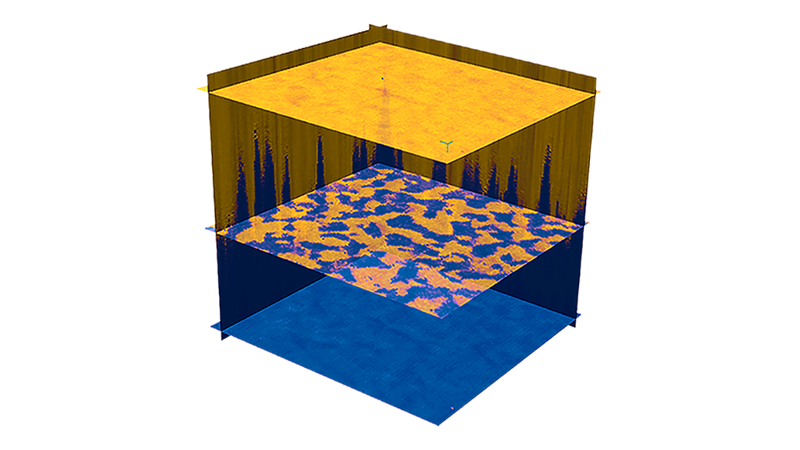
A second part covers three recent implementations providing more detailed insight in ferroelectric material properties: (i) The application of PFM methods in liquid environments including highly conducting liquids for life science and energy research. (ii) The combination of PFM with a DataCube approach providing a resonance spectrum in each pixel, maximizing sensitivity and at the same time avoiding the limitations associated with contact mode (as used with conventional implementations for PFM). (iii) Focus on quantitative measurements by a switching spectroscopy (SS-PFM) or contact Kelvin Probe Microscopy (cKPFM) approach to avoid artifacts in PFM point spectroscopy. Two of these will be illustrated with a short live demonstration.
[00:19:00] PRESENTATION 2
The Opportunities of functional material property mapping using Piezoresponse Force Microscopy | Dr. Nina Balke, ORNL
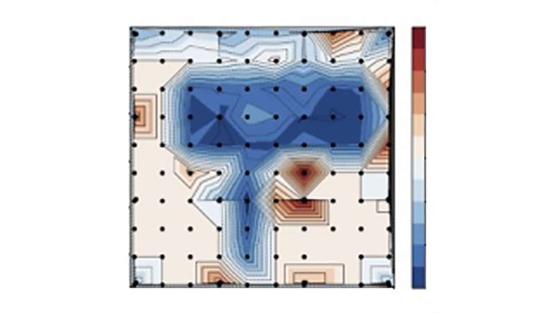
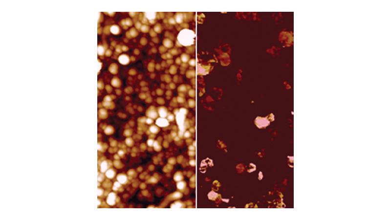
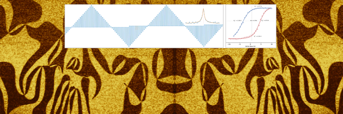
Piezoresponse Force Microscopy (PFM) has become a powerful tool to study local electromechanical sample responses in ferroelectric materials. PFM is used to image and manipulate ferroelectric domains in ceramics, thin films, and polymers and contains information about local piezoelectric properties (PFM amplitude) as well as the direction of the polarization (PFM phase) in the probed volume. However, the measured properties are often reported in arbitrary units and internal phase offsets make it necessary to shift the measured PFM phase which can result in a loss of physical information. This presentation will go over the fundamentals of PFM and will address the issue of unwanted signal origins and PFM phase corrections towards more quantitative measurements. The goal is to be able to measure and calibrate functional material properties which can be compared with macroscopic measurements or theoretical predictions for more in-depth insight into physical processes in the material. The successful combination of PFM and theory is demonstrated in a 2D layered ferroelectric material, CuInP2S6, which allows to greatly enhance the information gain obtained by PFM.
[00:54:30] PRESENTATION 3
PFM and Nano-PUND: Complementary Techniques for Ferroelectrics | Dr. Brice Gautier, INSA Lyon
Piezoresponse Force Microscopy (PFM) has become a standard for ferroelectricity assessment at the nanoscale. This presentation will review PFM operating modes including DFRT and introduce nano-PUND, a complementary approach. PFM signals can have origins other than ferroelectricity, especially in the case of very thin films, leaky samples, or when ionic conduction is possible. In some cases, proving the ferroelectric nature of a sample is not possible by PFM alone, and the added information from a complementary approach is needed.
At the macroscopic scale, PUND (Positive Up Negative Down) is used to measure the remnant polarization in leaky ferroelectrics. However, the application of the PUND method is particularly tricky because of the unfavorable signal to noise ratio: capacitive current appears to be several orders of magnitude higher than the current to be measured, not to mention additional leakage currents.
In this presentation, we show how PUND method can be used with an AFM tip as a top electrode, especially by compensating the spurious contributions (capacitive, leakage current): we have called it the nano-PUND method. We show examples of the implementation of nano-PUND and the advantages compared to PFM. Lead Zirconium Tantalate (PZT) is first used as a test material, then Hafnium Zirconium oxide (Hf0.5Zr0.5O2), extensively studied but particularly delicate when probed by PFM, illustrates the capabilities of the method.
[01:27:10] PRESENTATION 4
Recent Developments with Live Demonstration | Dr. Bede Pittenger and Dr. Mickael Febvre, Bruker
If you have any questions about our products or services, please contact us. Follow @BrukerNano on Twitter for event, product, and webinar updates.
This webinar was presented on: June 3, 2020
Speakers

Peter De Wolf, Ph.D., Director of Technology & Application Development
Peter De Wolf is director for AFM technology & application development at Bruker Nano Surfaces, covering all applications related to Scanning Probe Microscopy (SPM). He obtained his PhD from IMEC, Belgium on the development of new SPM methods for 2D carrier profiling in semiconductors and has more than 25 years of experience on SPM. He is the author and co-author of over 30 publications related to electrical characterization using SPM. He also owns several SPM patents, and developed several new SPM modes for electrical characterization.

Dr. Nina Balke
Staff Scientist, Oak Ridge National Laboratory
Nina Balke, received her Ph.D in Materials Sciences from the Technical University of Darmstadt, Germany, in 2006. After being a Feodor-Lynen fellow of the Alexander von Humboldt foundation at the University of California in Berkeley she transitioned to the Center for Nanophase Materials Sciences at Oak Ridge National Laboratory. She is specialized in nanoscale characterization of electromechanical effects in oxides and other functional materials focusing on ferroelectric and energy storage materials based on electro-chemo-mechanical coupling as well as in-situ characterization of solid-liquid interfaces.

Dr. Brice Gautier
Professor of Physics, Lyon Institute of Nanotechnologies
Brice Gautier is the head with Francis Calmon of the electronic devices team at the Institute of Nanotechnology of Lyon (INL), hosted by the national institute for applied sciences (INSA), where he teaches physics. He is involved in nanoscale electrical measurements using Atomic Force Microscopy, with the aim of characterizing semiconductors and thin oxides by e.g. scanning spreading resistance microscopy, scanning capacitance microscopy and conductive-AFM.
He has developped Piezoresponse Force Microscopy since 1999 for ferroelectric domains mapping and control. His past work has been focused on the reliability of electrical measurement using AFM, and in particular on the influence of water on dielectric breakdown and ferroelectric domain growth. His current research topics are focused on the control of ferroelectrics domains in thin films and single crystals with the aim of understanding the switching and growth of ferroelectric domains, and electrical properties of domain walls. Switching of domains by a mechanical stress is currently under study in PZT thin film.
Member of the CNANO network (french network focused on nanosciences), he is the president of the french nanometrology club (400 members, 30 % from the industry) devoted to the measurement at the nanoscale (http://club-nanometrologie.fr).