BioAFM Applications Gallery: Nanoscience
Atomic Resolution
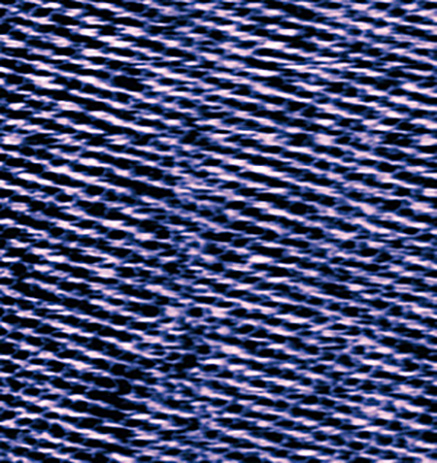
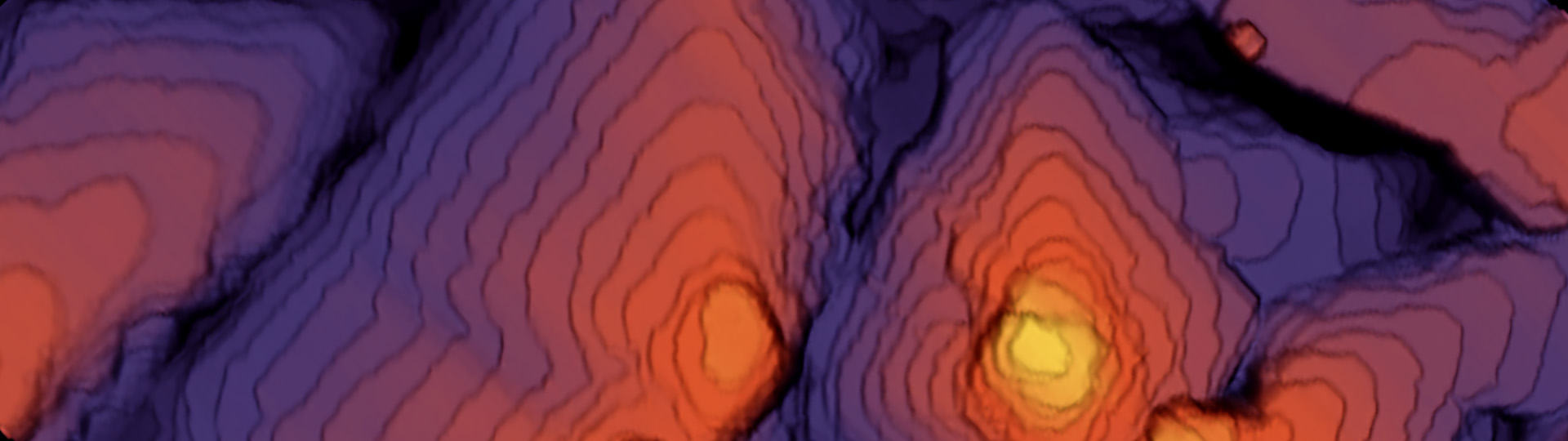
Atomic Resolution of Mica Taken on an Optical Microscope
Atomic resolution of mica in liquid, taken on a NanoWizard NanoScience AFM/optical microscope in closed-loop xy mode. Scan size: 13 nm x 13 nm.
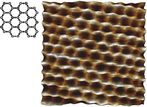
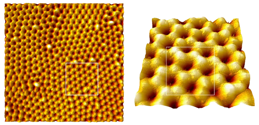
True Atomic Resolution of Mica
Crystal structure (left) and true atomic resolution image (right) of mica in liquid, 5 nm scan region, imaging in closed-loop xy mode. The hexagonal unit cell is clearly resolved.
Imaged with NanoWizard ULTRA Speed AFM.
Anorganic Surfaces
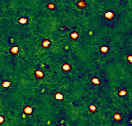
Gold Clusters in Water
AC mode height image of 20nm gold clusters imaged in water. The gold clusters were biotinylated and self-assembled on the surface. Imaged with a NanoWizard BioScience AFM. Scan field: 500 nm x 500 nm; Z-range: 25 nm.
Sample courtesy of:
C. Selhuber
Heidelberg University
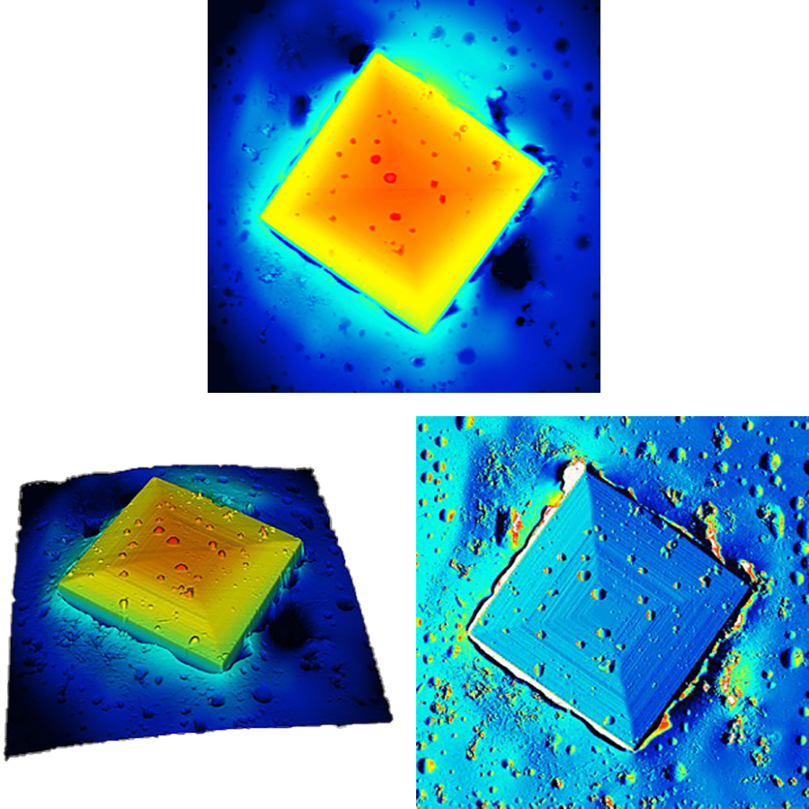
Zeolite Crystal
Height, amplitude, and 3D topography of a zeolite crystal, imaged with NanoWizard Sense AFM. The top surface of a zeolite crystal is embedded in a thermoplastic matrix. The crystal terraces can be seen on the surface.
- Top: Height image (scan field: 30 µm x 30 µm; z-range: 1 µm)
- Bottom left: 3D topography image (scan field: 30 µm x 30 µm)
- Bottom right: Amplitude image (scan field: 30 µm x 30 µm)
Sample courtesy of:
Prof. Anderson
University of Manchester, UK.
Anodic Aluminum
NanoWizard Sense AFM height image (3D plot) of an ordered pore array of aluminum (e.g., used as substrate for artificial lipid membranes). The pores were prepared by anodic etching in a self-organizing process.
- Left: Height image (scan field: 2 µm x 2 µm; z-range: 75 nm)
- Right: Height Image zoomed (scan field 500nm x 500 nm; z-range: 50 nm)
Sample courtesy of:
C. Steinem
Univ. of Regensburg
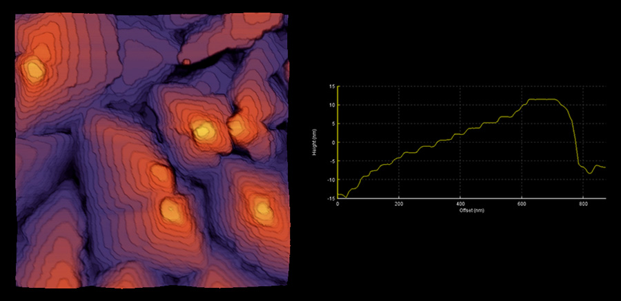
Oligomers and Nanofibers

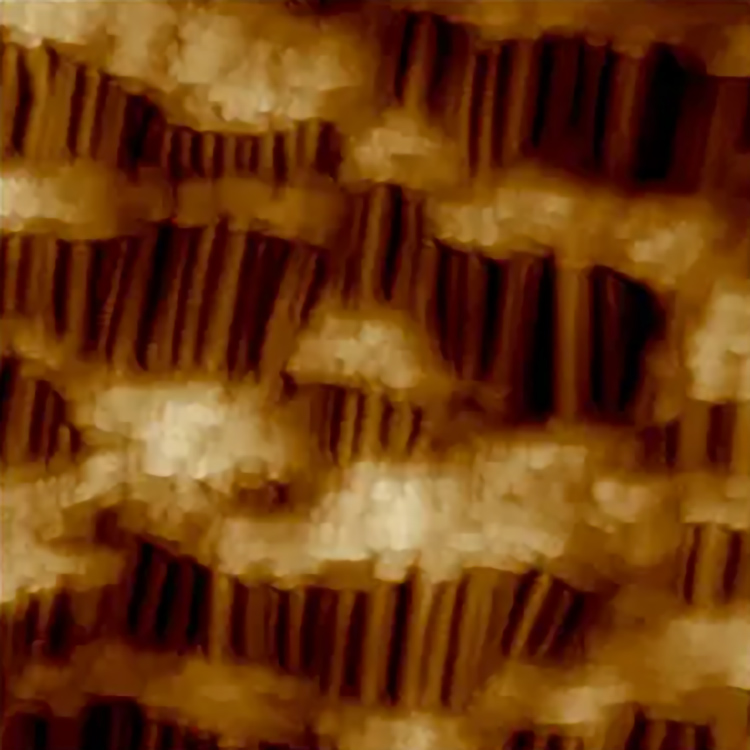
Hexacontane
Hexacontane C60H122 prepared on HOPG. Adhesion image (range: 2 nN) measured with a NanoWizard NanoScience AFM in QI™ mode. Stripes are monomolecular layers of Hexacontane.
Scan size: 250 nm × 250 nm, xy-closed loop.
Layers and Thin Films
Pentacene Layers
Island growth of pentacene layers on silicon. Scan size: 2 µm x 2 µm, z-range: 29.5 nm. Taken on a NanoWizard NanoScience AFM.
- Left: 3D topography image
- Right: Cross-section
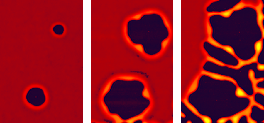
Melting of a Thin Film of Polystyrene
Melting and dewetting of a thin film of polystyrene on silicon over 40 minutes, using JPK Heating Cooling Stage - HCS™ to maintain the temperature at 45 °C. Imaged with NanoWizard NanoScience AFM.
Scan size: 4 µm x 6 µm, z-range: 56 nm.
Crystalline Polyethylene at -120°C
Topography image of crystalline polyethylene measured at -120°C with JPK Cryostage on a NanoWizard NanoScience AFM.
- Left: Scan size: 2 μm × 2 μm; z-range: 15 nm
- Right: Scan size: 1 μm × 1 μm; z-range: 15 nm
PTFE (Teflon™) Layer
Topography and elasticity of a PTFE (Teflon™) layer, imaged with NanoWizard NanoScience AFM in QI™ mode.
- Top: Height image (Scan size: 10 µm × 10 µm; Z-range: 1.4 µm)
- Bottom left: Elasticity image (Scan size: 10 µm × 10 µm; Elasticity range: 350 MPa)
- Bottom right: 3D topography overlaid with elasticity (Scan size: 10 µm × 10 µm)
Sample courtesy of:
Adam Mickiewicz University
Poznan, Poland
Langmuir Blodgett Film
NanoWizard NanoScience AFM height and phase images of a Langmuir Blodgett film. Scan field: 5 µm x 5 µm; Z-range: 10 nm
- Left: Height image
- Right: Phase image
Celgard® Fast Scanning
Topography image of Celgard® with scan size 1 µm, 23 Hz line rate. Imaged with NanoWizard ULTRA Speed AFM. Scan size: 1 µm × 1 µm, Z-range: 100 nm.
Particles and Capsules

Microrheology on Silica Beads
Microrheology on silica beads (d = 2 μm) partially embedded into PDMS: Overlay of topography (grayscale) and loss modulus G‘‘ (color texture) recorded at a modulation frequency of 100 Hz. Imaged with a NanoWizard NanoScience AFM
Scan size: 15 μm x 15 μm.
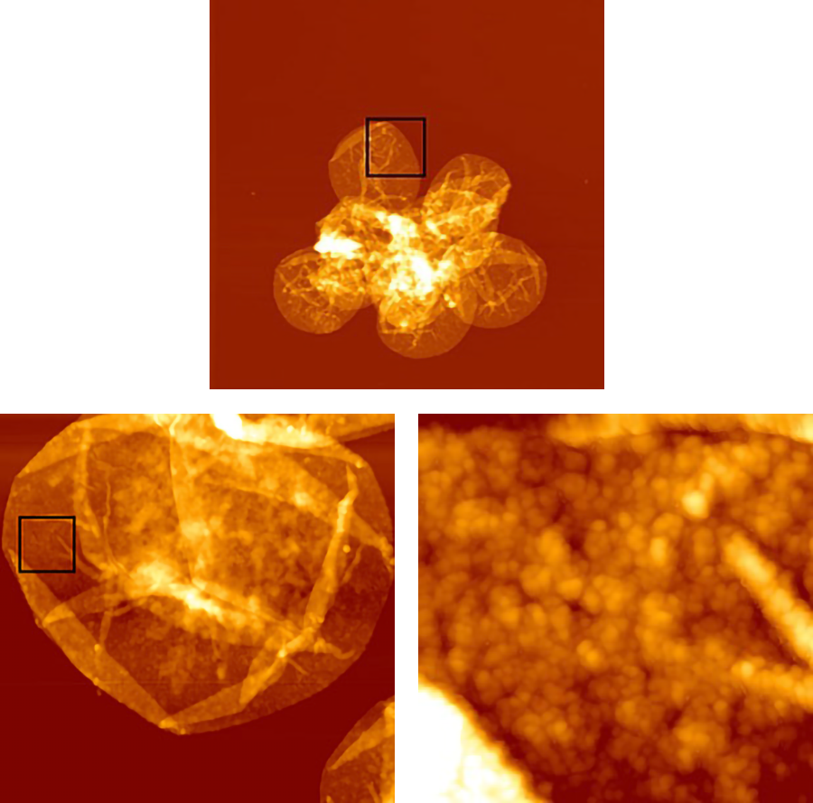
Hollow Microcapsules
Height images (2 samples) of hollow microcapsules (PSS/PAH), imaged in air with the NanoWizard NanoScience AFM.
- Top: Height image (sample 1) (Scan field: 22.9 µm x 22.9 µm; Z-range:350 nm)
- Bottom left: Height image (sample 2) (Scan field: 7.5 µm x 7.5 µm; Z-range: 400 nm)
- Bottom right: Height image zoomed (sample 2) (Scan field: 1 µm x 1 µm; Z-range: 0-80 nm)
Sample courtesy of:
E. Donath, Leipzig University
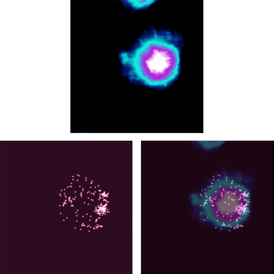
Recognition Microscopy on Biotin Bead
Recognition microscopy on biotin bead (diameter 200 nm) against streptavidin functionalized cantilever, performed on a NanoWizard BioScience AFM. Force-distance curves were processed to evaluate for the typical biotin-streptavidin binding signature for binary recognition image reconstruction. Scan size: 375 nm × 375 nm.
- Top: Height image (z-range: 50 nm)
- Bottom left: Binary recognition image, bright spot indicates a binding event
- Bottom right: Overlay of height and recognition