Technical Note: ScanningWear – Measuring Wear Resistance at the Nanoscale
Wear resistance testing with ScanningWear™
ScanningWear™ testing is a feature enabling research into wear resistance of coatings and films at the nanoscale. The capability is standard on all Hysitron® TS and TI Series instruments, providing a complementary technique to nanoindentation and scratch.
How ScanningWear Works
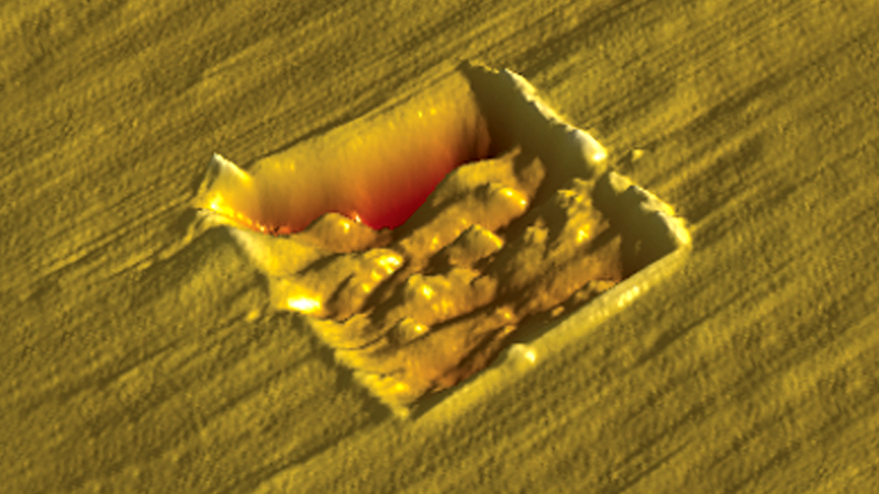
The wear patterns are created by raster scanning the sample with a given force, predefined by the user. A scan can consist of a single pass or multiple passes over the same area within one test. By applying a known force and selecting the number of passes over which this force is applied, the amount of material that is removed during the wear scan can be measured post-test using the in-situ imaging technique.
ScanningWear enables the ability to wear at different loads and carry out several wear experiments on one sample, as show in Figure 1. This experiment involved several individual wear tests carried out at increasing loads and number of passes on a hard drive’s DLC film coating. The amount of material removed in each wear test was measured using in-situ imaging (see Figure 2).
The precise positioning that in-situ SPM imaging provides also enables nanomachining and nanopatterning on surfaces, as shown in Figure 3. In this study, two wear patterns were nanomachined in lanthanum oxide. One pattern consisted of a 5 µm x 5 µm square, the other a 1.25 µm x 5 µm rectangle. The patterns were placed less than 1 µm apart, the oxide layer was removed to selectively reveal the substrate.
ScanningWear Features
- Programmable forces for precise load control within a wear box
- Adjustable wear track size from <1 µm to 100 µm
- Single- or multiple-pass wear testing capabilities
- Wear volume easily measured using in-situ SPM imaging
- Roughness measurement utility as standard
- Sensitivity to measure <1 nm of material removal
- Ability to test in fluid mediums, such as lubricants and oils
Applications
- Nanomachining: Perform mechanical contact machining with sub-micron accuracy
- Lubrication: Study wear characteristics on materials with and without lubricants for failure prediction
- Additive Performance: Study the effect on performance due to the addition of functional additives
- Effects of Oxides: Investigate wear of surface oxide layers to find the effect they have in protecting material surfaces
- Sliding Contact: Perform unidirectional wear studies to understand sliding contact effects on material failure
- Protective Coatings: Study the wear resistance of protective coatings
Hysitron and ScanningWear are trademarks of Bruker Corporation. All other trademarks are the property of their respective companies. © 2019 Bruker Corporation. All rights reserved. TN1502, RevA0.

