
Bruker Nanoindentation User Meeting 2026
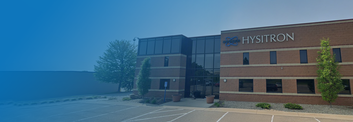
Bruker is pleased to announce the Bruker Nanoindentation User Meeting 2026 from June 9 – 10 in our Eden Prairie, MN facility. This event will include discussions on the latest developments in nanomechanical and nanotribological testing technology, presentations on applied testing, hands-on training, a tour of the facility, and a poster showcase with applications discussion.
Don’t miss this opportunity to:
- Discover new trends in nanomechanical and nanotribological testing
- Build your nanomechanical testing skillset with hands-on training alongside Bruker’s applications team
- Engage with Bruker’s presentations, colleagues, and a poster showcase
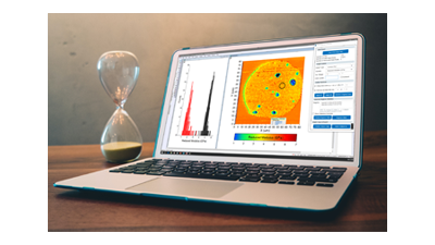
Instructional tutorial topics will include advanced nanomechanical techniques, including XPM property mapping and automation, nanoDMA, nanoscratch, testing in extreme environments, in‑situ testing in SEM/TEM, testing biomaterials, and more.
Participation fee:
- Professional: $300
- Academic: $150
**THIS EVENT HAS REACHED CAPACITY**
Agenda
Day 1 – Technology, Applications & Facility Tour
Time | Session | Description | Speaker |
8:30 – 9:00 | Registration & Coffee | Badge pickup and networking | |
9:00 – 9:15 | Welcome & Meeting Overview | Bruker Nano Surfaces leadership introduction | Sanjit Bhowmick, David Vodnick |
9:15 – 9:45 | Bruker Facility Tour | Manufacturing, applications labs, and demonstration facilities | |
9:45 – 10:15 | Technology Update | Latest developments in automation, property mapping, and instrumentation | David Vodnick |
10:15 – 10:30 | Coffee Break | — | |
10:30 – 11:00 | Tutorial – XPM Property Mapping | High-throughput nanomechanics and automation workflows | Eric Hintsala |
11:00 – 11:30 | Application Talk – Soft Materials & Biomaterials | Dynamic mechanical analysis for polymers and biomaterials | Radhika Laxminarayana |
11:30 – 12:00 | Special Session 1 – Tribometer and Mechanical Testing | Evaluating Friction and Wear Behavior of Engineered Plastics Using Thrust Washer Tests | Sai Kancharla |
12:00 – 1:00 | Lunch | — | |
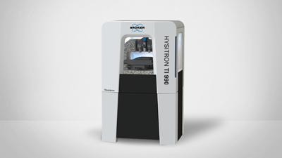
1:00 – 2:30 | Hands-On Instrument Rotations | - TI 990 operation | |
2:30 – 2:45 | Coffee Break | — | |
2:45 – 3:45 | Advanced Tutorial – Extreme Environment Testing | From Cryo to High Temperature and environmental testing methods | Kevin Schmalbach |
3:15 – 3:45 | Special Session 2 – AFM & Nanoindentation Correlation | Connecting PeakForce Tapping with nanoindentation measurements | Ilias Halimi, Hikari Kitadai |
3:45 – 4:45 | Keynote | Future directions in nanomechanical and nanotribological testing | |
4:45 – 6:00 | Poster Session & Networking Reception | Posters, discussions with Bruker scientists |
Day 2 – Advanced Methods & Training
Time | Session | Description | Speaker |
8:30 – 9:00 | Coffee & Networking | — | |
9:00 – 9:10 | Day 2 Welcome | Agenda recap | Hikari Kitadai |
9:10 – 9:40 | Keynote Talk | A Nanoindentation-based method for predicting creep rupture in Nuclear Reactor Steels | Prof Nathan Mara |
9:40 – 10:10 | Advanced Application Talk | Fracture and delamination of thin films and coatings | David Vodnick |
10:10 – 10:30 | Coffee Break | — | |
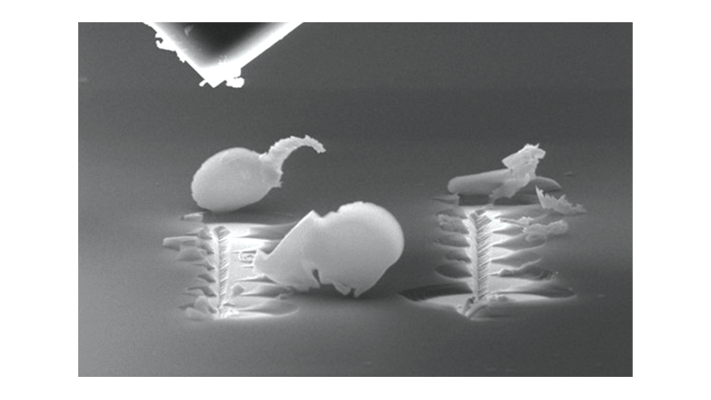
10:30 – 11:30 | Technical Talk – In-Situ Nanomechanics | Mechanical testing inside Electron Microscopes | Sanjit Bhowmick |
11:30 – 12:00 | Expert Panel Discussion | Best practices in nanomechanical testing | |
12:00 – 1:00 | Lunch | — | |
1:00 – 2:30 | Advanced Training Sessions | Track A Advanced Methods Track B Data Analysis | |
2:30 – 2:45 | Coffee Break | — | |
2:45 – 3:45 | Open Lab Session | Instrument demonstrations and experiment discussions | |
3:45 – 4:15 | Poster Awards | Best student and application posters | |
4:15 – 4:30 | Closing Remarks | — | |
4:30 – 6:00 | Optional Networking / Instrument Demos | Continued discussions and demos |
Meet the Team


Meeting Venue
The Eden Prairie, MN facility is conveniently located 20 minutes from the Minneapolis-St. Paul International Airport (MSP). To see directions from MSP to the facility on Google Maps, click here.

9625 West 76th St., Eden Prairie, MN 55344
Call for Posters
We invite researchers and users to submit a poster abstract highlighting their work, applications, or innovations using Bruker Nanoindentation (NI) technologies. Selected submissions will be invited to present a poster during the User Meeting poster sessions.
**POSTER SUBMISSIONS ARE NOW CLOSED.**
Registration
This event has reached capacity.