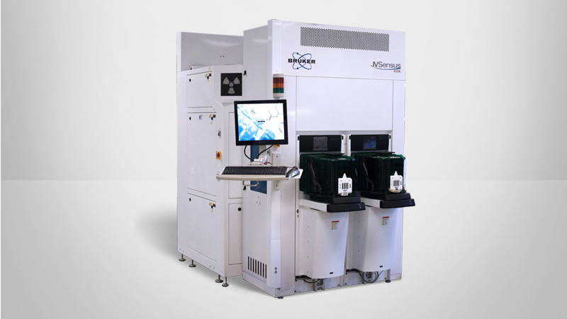
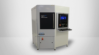
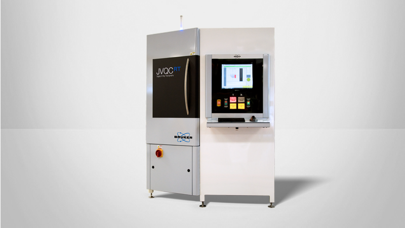
X-Ray Defect Inspection
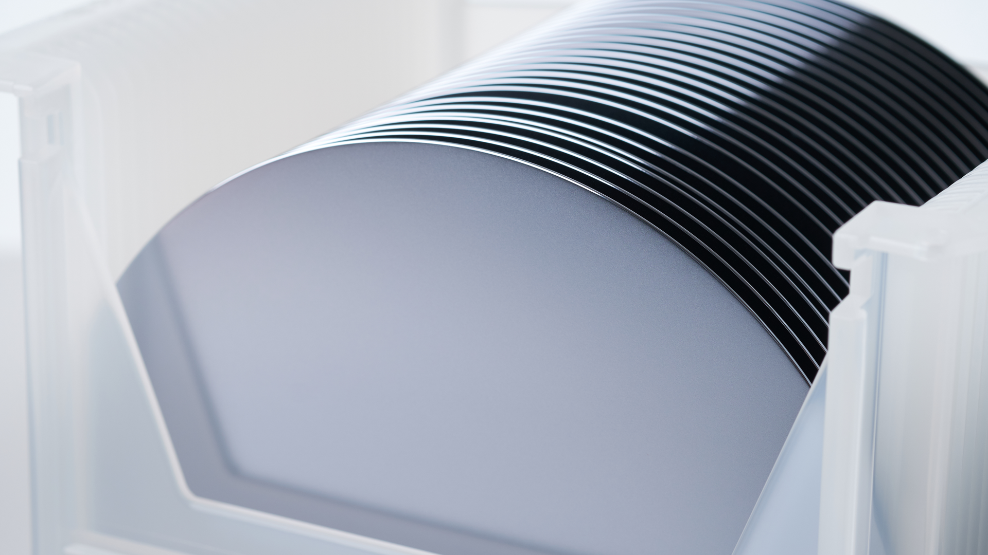
Bruker defect detection systems use X-ray diffraction imaging (XRDI) to detect crystalline defects, such as cracks, slip, dislocations, and micropipes on single-crystal substrates. Our XRDI inspection technology operates without the use of etching acids. These systems are broadly employed to detect cracks in Si wafers that cause wafer breakage and to improve yield and quality of other high-value substrates, such as CdTe and SiC.
Support

How Can We Help?
Bruker partners with our customers to solve real-world application issues. We develop next-generation technologies and help customers select the right system and accessories. This partnership continues through training and extended service, long after the tools are sold.
Our highly trained team of support engineers, application scientists and subject-matter experts are wholly dedicated to maximizing your productivity with system service and upgrades, as well as application support and training.