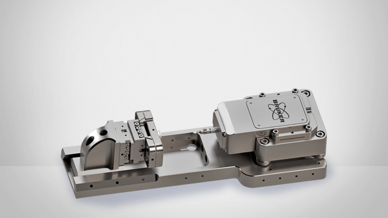
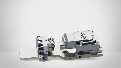
Electrical Characterization Module
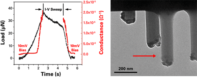
Bruker’s Electrical Characterization Module (ECM) for the PI Series instruments provides a powerful solution for simultaneous in-situ electrical and mechanical measurements. Using a conductive path that connects the probe and sample, a voltage bias is applied to allow continuous measurement of evolving electrical contact conditions as a function of applied force and probe displacement. Site-specific testing can be performed by confirming proper tip placement with electron microscope imaging. Through-tip electrical measurements can also be used to gain insight into electromechanical properties of micro- or nano-structures such as pillars and particles. Humidity or water adsorption effects are minimized by the vacuum environment of the electron microscope.
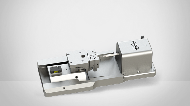
Furthering the capabilities of ECM, a MEMS Electrical Push-to-Pull (E-PTP) device enables tensile testing while simultaneously measuring sample resistivity using a standard four-point measurement. The separation of current sourcing and voltage sensing electrodes allow accurate measurements of the electrical properties by elimination of contact and lead resistance on the measurement. Voltage sweeps can also be performed to measure IV curves, while true stress and strain are determined by monitoring and measuring specimen dimensions in the electron microscope.