Application Note: In-Situ Electromechanical Testing of ZnO Nanowires
Evaluating Electromechanical Properties of ZnO Nanowires using Electrical Push-to-Pull Technology
One-dimensional structures such as nanowires and nanotubes are potential materials for future nanoelectronics, optoelectronics, piezoelectric devices, sensors, and actuators. Due to length scale effects and higher surface-to-volume ratios, nanostructures can exhibit superior mechanical and electrical, as well as other length scale dependent properties. To utilize these fundamental advantages, it is essential to investigate and understand their unique characteristics as a function of the material parameters. In spite of the great technological progress that has been made during the last decade, comprehensive electromechanical characterization of a single individual nanowire is still a demanding task.
KEYWORDS: Electromechanical Testing; Nanowires; Electrical Push-to-Pull; Tensile Testing; PI 85L; SEM PicoIndenter; I-V Curves; Resistivity
Electrical Push-to-Pull (E-PTP)
A MEMS-based uniaxial nanotensile testing device with integrated four-probe electrical contacts has been designed for electromechanical characterization of materials
(Figures 1–4). The small size of the E-PTP device, (2.5 mm x 2 mm x 0.4 mm), in conjunction with Bruker’s Hysitron® PI Series PicoIndenter® instruments, allows for direct-observation of the deformation process in TEM and SEM.
E-PTP Features and Benefits
E-PTP devices offer a number of benefits for simultaneous in-situ electical and mechanical measurements.
- E-PTP device enables tensile testing of individual nanowires with high resolution of the force and displacement, simultaneously measuring electrical properties by the four-point probe method.
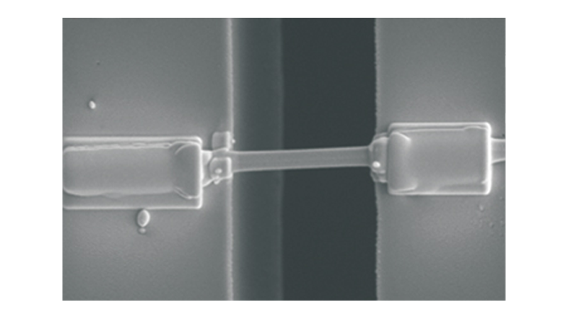
- Sample mounting involves picking and placing a nanowire with a nanomanipulator on the flexure. The nanowire is then welded across the 2.5 µm gap.
- Separation of current-sourcing and voltage-sensing electrodes allow accurate measurements of the electrical properties by eliminating contact and lead resistance on the measurement.
- Uniaxial tensile testing with the E-PTP avoids substrate effects and applies a uniform deformation field along the length of the sample.
- I-V curves generated during the mechanical test aid in the correlation of electrical to mechanical transitions in a material.
- E-PTP devices with Hysitron PI Series PicoIndenter instruments aid in understanding the microscopic origin of electrical property changes in the sample under loading.
ZnO Nanowire on E-PTP
Non-centrosymmetric wurtzite structure zinc oxide (ZnO) exhibits a strong piezoelectric tensor among tetrahedrally bonded semiconductors, and is a promising material for sensors, actuators, and energy harvesting applications. In this study, uniaxial tensile tests with a four-point probe electrical measurement were performed via E-PTP to understand the piezoelectric response of ZnO as a function of strain. Nanowires of ~300 nm diameter and ~20 micron length were placed on a E-PTP inside a dual-beam SEM-FIB. Pt-based gas injection system (GIS) was used for welding and for connecting four leads to the sample as shown in Figure 3 (left).
In-Situ E-PTP Experiments
The Hysitron PI 85L SEM PicoIndenter (learn about the new model of this system) in Electrical Characterization Module (ECM) mode was used to conduct strain-rate controlled tensile experiments inside an FE SEM. A Keithley 2602A SourceMeter was used for sourcing current and measuring voltage in four-probe mode. Voltage sweeps at constant strain were performed to obtain I-V curves in order to extract electrical properties. Periodic stress or strain from the nanowires was generated by periodic variation of the applied voltage or current. One of the advantages of the in-situ study is that instantaneous length and diameter of the nanowire can be measured from video frames and correlated with mechanical response. True stress and true strain were determined using force-displacement data and plotted in Figure 3 (right). The actual force to the nanowire (Psample) was determined by subtracting the force calculated using the spring stiffness of the E-PTP (PE-PTP) from the experimentally measured load (P), i.e., Psample = P–PE-PTP. The stiffness of this E-PTP device was measured after the fracture of the nanowire and found to be 320 N/m.
Piezoelectric Effect in Tensile Loading
In all the experiments, ZnO nanowires showed steady increase in current (i.e., decrease in resistance) with a specific applied voltage during loading as shown in Figure 3 (right). In non-piezoelectric materials, one can expect an increase in electrical resistance in tensile loading as the length of the nanowire increases and diameter decreases. The non-linear stress-strain curve in the elastic tensile regime of ZnO also indicates that the mechanical response is influenced by piezoelectric effect of the nanowire. The elastic modulus of ZnO was calculated to be ~88 GPa from a separate set of experiments where no voltage was applied.
Resistivity was calculated from the linear I-V curves, Figure 4 (left), as a function of tensile strain. The piezoelectric response curve in Figure 4 (right) shows a fluctuation in stress generated by applied voltage steps, while the nanowire is held at a constant 2.2% true strain. A finding of particular interest is that the change in stress generated by voltage fluctuation, .s(V) , depends on the amount of tensile strain (eT) applied to the nanowire, and .s(V) is directly proportional to eT. Besides the strain-induced mobility enhancement as observed in silicon and other semiconductor materials, another possibility is that the piezoelectric potential across the nanowire length is influenced by tensile elongation, which in turn significantly modifies the electrical transport properties.
Conclusion
This in-situ electromechanical study demonstrates a novel approach to understand direct piezoelectric response of ZnO nanowire. E-PTP technology can also help to understand how phase transformation, defects, large-strain plasticity, crystallographic, and grain boundaries orientation, and size influence mechanical and electrical properties of nanomaterials.
Bruker Nano Surfaces Division is continually improving its products and reserves the right to change specifications without notice. Hysitron and PicoIndenter are trademarks of Bruker Corporation. All other trademarks are the property of their respective companies. © 2017 Bruker Corporation. All rights reserved. AN1502, Rev. A0

