Hysitron PI Envision SEM PicoIndenter

Hysitron PI Envision SEM PicoIndenter
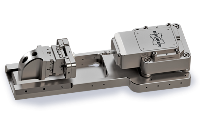
Hysitron PI Envision is a leading-edge nanomechanical testing instrument designed for in-situ operation in standard SEMs, FIB-SEMs, small-chamber SEMs, and even synchrotron beamlines. Its sub-nanometer displacement and sub-micronewton resolution make it suitable for analyzing materials from soft polymers to high strength metals and alloys. This modular platform is highly upgradable, supporting a powerful suite of techniques, including nanoindentation, property mapping, and high-temperature testing up to 800°C. PI Envision delivers best-in-class versatility, precision, and value ideal for multi-user facilities and budget-conscious laboratories.
To learn more, continue reading, download the brochure, or see FAQs about this product.
Affordable, Reliable, Upgradable, and Easy to Use

Hysitron PI Envision is an easily upgradable platform that offers a powerful suite of in-situ testing techniques. It is an indispensable, affordable, and reliable SEM accessory for nanomechanical and nanotribological testing.
PI Envision delivers:
- Intrinsic displacement control, intrinsic load control, and open loop nanomechanical testing for a wide range of materials
- Advanced upgrades for performing nanotribology, property mapping, and high-temperature testing to 800°C
- Encoded stage control and 78 kHz feedback rate for fast, repeatable results from indentation, compression, tension, or fatigue testing
The PI Envision SEM PicoIndenter enables intuitive, spatially clear in-situ nanomechanical testing within the SEM with efficient setup, direct sample observation, and controlled interaction.
Key features include:
- Actuation and sample side separation clearly defining how force is applied and how the sample is positioned, helping users understand and control interaction within the SEM
- In-situ nanomechanical testing within the SEM enabling observation of the sample during interaction as part of the testing workflow
- Clear system layout making component positioning and relationships easy to interpret, reducing ambiguity and supporting more efficient setup
- Guided, step-by-step introduction showing how users begin interacting with the system and progress from initial setup into testing through a structured walkthrough
Essential Ease-of-Use Features
PI Envision is designed to streamline your work, with:
- An encoded stage to ensure precise sample positioning
- Positioning travel of 12x12 mm to provide easy sample access
- No-stitch property mapping for >1 mm x >1 mm area
- Two sample mounts to reduce manual sample changes

Configure Your System
All PI Envision configurations deliver intrinsic displacement actuation and control with sub-nanometer resolution, feedback rate of 78 kHz, and data acquisition up to 39 kHz.
The base system supports up to 10 mN force and sub-nanometer to 5 µm displacement range, making it an excellent choice for routine indentation, compression, and tensile testing of low-hardness to medium-hardness materials.
An optional xR transducer extends the maximum load to 250 mN and displacement range up to 100 µm, making it ideal for high-hardness materials and nanotribology.


Additional testing capabilities include:
- Push-to-Pull (PTP) Tensile Testing — Uniquely simplifies tensile testing of nanostructures such as nanotubes, nanofibers, nanowires, and thin films
- Electrical PTP Tensile Testing — Enhances PTP testing with integrated four-point electrical measurements to study electromechanical coupling
- Electrical Characterization — Monitors changes in electrical properties during mechanical deformation; applicable to piezoelectric and other functional materials
- nanoDynamic Testing — Applies oscillatory forces to continuously evaluate viscoelastic and fatigue properties at room and elevated temperatures


Key features and specs of PI Envision and PI 89
| PI Envision | PI 89 | |
| Max transducer force (mN) | 250 mN | 3500 mN |
|---|---|---|
| Max transducer displacement | 100 µm | 150 µm |
| Stage travel (X, Y and Z), Y = indentation direction | 12, 16, 12 | 26, 29, 12 |
| Sample position (XY) | 12 mm x 12 mm | 12 mm x 26 mm |
| Multi-Sample mounting compatibility | 2 samples | 6 samples |
| Property mapping area | 12 mm x 12 mm | 12 mm x 26 mm |
| High temperature | 800°C | 800°C and 1000°C |
| Rotation and tilt stage (5 deg of freedom for in-situ correlative characterization) | No | Yes |
| Cryogenic temp | Not available | -130°C (possible to reach well below -130°C depending on the sample size and SEM chamber) |
| nanoTribology | Yes | Yes |
| Push-to-Pull and Electrical; Push-to-Pull | Yes | Yes |
| NanoDynamic, Fatigue | Yes (room temperature and high temperature) | Yes (room temperature, high temperature and cryogenic temperature) |
| Electrical characterization | Yes | Yes |
| DOWNLOAD THE BROCHURE TO SEE FULL SYSTEM SPECIFICATIONS |
Analyze Your Data
Hysitron nanomechanical test instruments come standard with Tribo iQ, Bruker’s complete data processing, graphic, and reporting solution. Tribo iQ encompasses a suite of technique-specific software applications that simplify and streamline the experiment-analysis loop.


Frequently Asked Questions
PI Envision is highly upgradable, supporting a powerful suite of techniques, including nanoindentation, compression testing, tension testing, fatigue testing, property mapping, nanotribology, and high-temperature testing up to 800°C.
Transducers and flexures are interchangeable components of PI Envision. It has extended force options up to 250 mN and displacement up to 100 µm.
PI Envision is not compatible with the rotation and tilt (R/T) stage, meaning that it is also not compatible with seamless switching between nanomechanical testing and EBSD imaging. For this capability, we recommend PI 89 Auto.
High‑temperature testing up to 800 °C and nanoScratch are available as configured options.
PI Envision is not compatible with cryogenic testing. For low-temperature testing, we recommend PI Cryo.
PI Envision supports automated property mapping with encoded positioning and area coverage up to 12 mm x 12 mm. No-stitch property mapping is possible for >1 mm x >1 mm area.
PI Envision offers a broad catalog of tips in multiple geometries and materials, including diamond, sapphire, vanadium carbide, boron nitride, tungsten, and steel. Contact us for help selecting the appropriate tip for your research.
Yes. You can request a quote using our online form, or contact us directly.
Contact Us About the Hysitron PI Envision SEM PicoIndenter
Ask us a question, request more information, or get in touch with a Bruker sales representative.