Virtual Event, Actual Science

Maximizing Process Efficiency and Yield with High-Performance Metrology Techniques:
A Two-Part Webinar Series

Learn how Bruker’s in-line and lab-based metrology solutions accelerate and improve semiconductor R&D and manufacturing processes

Pick the best metrology technologies for your R&D, process control, failure analysis, and reliability testing needs.

In this on-demand two-part webinar series, you will learn how to apply Bruker’s high‑performance metrology techniques to evaluate and optimize front-end processes, back-end processes, and failure analysis. Our team of application experts use case studies to demonstrate where Bruker’s benchtop and automated metrology solutions can add capability and value.

PART 1:
Accelerating Front-End Semiconductor Process Control with Accurate Metrology and Characterization

Discover how Bruker's benchtop and automated metrology solutions can improve and optimize your semiconductor front-end process control and yield management.

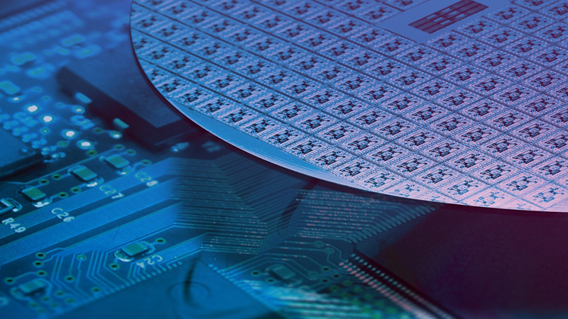
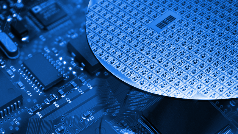
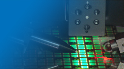
Bruker's high-performance metrology and characterization techniques can provide new insights for your R&D or process control by assisting in the nanometer-scale surface evaluation of semiconductor materials and devices. During Part 1 of this series, our applications experts discuss and demonstrate how each of our core technologies can be applied to the most current technology nodes and wafer processing steps in front end, back end, and failure analysis areas. Presentations include case study examples showcasing the specific uses and advantages of each technology.

PART 2:
Scanning Probe Microscopy and Nano-Indentation for Semiconductor Failure Analysis and Reliability

Part 2 of this series addresses how scanning probe microscopy (SPM) and nanoindentation can advance failure analysis and reliability testing in the semiconductor industry.

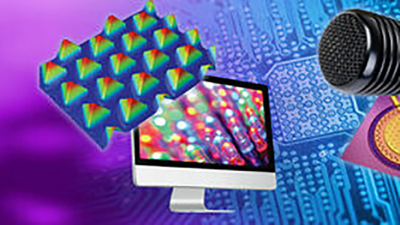
SPM, or atomic force microscopy (AFM), is known for its ability to image surface topography with nanoscale spatial resolution, but its capabilities extend much further. By choosing the right probes, modes, and methods, SPM can be adapted to measure a variety of electrical, magnetic, thermal, and mechanical properties. More recently, SPM has also been expanded to enable chemical identification at the nanometer scale using AFM-IR methods. In the first half of this segment, Bruker experts use Si and compound semiconductor device examples to demonstrate how standard topographical AFM imaging and other types of property imaging can be used to inform semiconductor failure analysis and improve reliability.

The second half of this segment focuses on how nanoindentation can be used for quantitative nanomechanical characterization and in-situ (inside the SEM or TEM) direct observation in semiconductor applications. Bruker experts present nanoindentation case studies — including the thermal expansion of Cu-TSVs — to demonstrate our nanomechanical test instruments' broad suite of complementary characterization techniques and how they can be leveraged for semiconductor failure analysis and reliability testing.

Input value is invalid.

Submit the Form for Instant, Full-Length Access

* Please fill out the mandatory fields.

Please enter your first name
Please enter your last name
Please enter your e-mail address
Please enter a valid phone number
Please enter your Company/Institution
What technology are you most interested in?
What best describes your current interest?
Please add me to your email subscription list so I can receive webinar invitations, product announcements and events near me.
Please accept the Terms and Conditions

             Privacy Notice   Terms of Use


Note: Page will refresh upon submission; afterward, you may need to scroll down to see the video access link.

Webinar Recording is Now Available.


Note:
If you close or exit this page, you will not be able to reopen this confirmation window without re-submitting the form. Please save these access links to bypass the form in future visits.

Related Webinars

Characterization-of-semiconductors-webinar-teaser-BRUKER
On Demand • 2 Hrs

Surface Characterization of Semiconductors: An Overview, from Topography to Advanced Physical Properties

Watch exclusive expert lectures and live demonstrations of Bruker’s high-performance metrology technology and the latest techniques for the nanometer-scale surface characterization of semiconductor materials and devices.
Macro of Silicon Wafers 713206981
On-Demand | 2 Hrs 55 Min

Surface Characterization of Semiconductors Workshop [2021]

Discover Bruker's complete range of high-performance metrology solutions for the nanometer-scale surface characterization of semiconductor materials and devices.
Application of Atomic Force Microscopy in the Study of Semiconductor Materials and Devices
On-Demand Session | 65 Minutes

Application of AFM in the Study of Semiconductor Materials and Devices

Explore the ways that AFM can assist in the nanometer-scale characterization of semiconductor materials and devices, especially electrical characterization.
Advanced 3D Optical Metrology
On-Demand Session • 50 Minutes

Accelerating Semiconductor Processes Control with Advanced 3D Optical Metrology

Discover recent advancements in 3D Optical Metrology and how they accelerate in-line quality control for both front- and back-end processes, supporting next-generation semiconductor device development.
Thin Film Characterizations Applied in Semiconductor Industries
Webinar Recording • 1 Hr

Thin Film Characterizations Applied in Semiconductor Industries

Hear about current challenges in thin film mechanical property analysis and techniques that offer significant benefits for such problems.
Select "Image is decorative" unless given very specific details as caption
On-Demand Session • 45 Minutes

Thin Film Characterization Using Spectroscopic Reflectometry and Ellipsometry Techniques

See how our unique and proprietary polarized light techniques support film thickness, morphology, and optical properties research, production, and QA/QC across industries.
Input value is invalid.

Contact Us

* Please fill out the mandatory fields.

Please enter your first name
Please enter your last name
Please enter your e-mail address
Please enter a valid phone number
Please enter your Company/Institution
What technology are you most interested in?
What best describes your current interest?
Please add me to your email subscription list so I can receive webinar invitations, product announcements and events near me.
Please accept the Terms and Conditions

             Privacy Notice   Terms of Use

Thank you

Your request was successfully sent.

You can email us with more information at productinfo@bruker.com.


If you would like to connect with a Bruker representative immediately, here are our regional offices:

Asia: +65 6540 4388
China: +86 10 5833 3000
Europe: +33 172 86 61 00
Japan: +81 3 3523-6361
North America: +1 805-967-1400