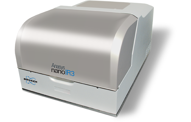
Anasys nanoIR3
Anasys nanoIR3
The nanoIR3 is the latest generation nanoscale IR spectroscopy, chemical imaging, and property mapping system for both materials and life science applications. The system also provides IR-based chemical imaging to provide mapping of chemical variations of the feature of interest. Unique point spectroscopy capabilities provide both spectroscopy and chemical imaging with a single source.
To learn more, continue reading, contact us, or see FAQs about this product.
Complete Nanoscale Characterization
The nanoIR3 provides a comprehensive set of capabilities for nanoscale characterization. The unique POINTspectra feature provides both point spectroscopy and chemical imaging with a single laser source, enabling faster time to data and, ultimately, a more cost-effective research solution. Hyperspectral Imaging provides the ability to create a 3D spectral map of the surface within to help identify unknowns and export for additional processing.
High-Performance Monolayer Sensitivity
Bruker’s proprietary Resonance-Enhanced AFM-IR mode provides the highest performance, rich, high-quality spectra to help identify materials at the nanoscale and better understand material changes and composition. From thin films to monolayers, Resonance-Enhanced AFM-IR is the most sensitive technique for nanoscale spectroscopy of organic materials.
Tapping AFM-IR Chemical Imaging
Incorporating proprietary technology and building upon years of industry-leading Anasys AFM-IR instrument development, the nanoIR3 is the highest performance nanoscale IR. Our patented Tapping AFM-IR imaging technique creates chemical mapping of the highest spatial resolution, while providing high-quality IR spectroscopy, chemical imaging, and materials property mapping system available today for materials and life science applications. Whether your goal is creating chemical composition maps of polymers, thin films, monolayers, or small, thin contaminants, obtaining high-resolution chemical imaging is easy and fast with Tapping AFM-IR.
nanoIR3 for Nanoscale Chemical and Surface Analysis
The nanoIR3 supports nanoscale chemical analysis and materials characterization by combining atomic force microscopy with infrared spectroscopy. It is used across materials science and life science research to correlate surface structure, material properties, and chemical composition at nanometer-scale resolution, with direct correlation to FTIR spectroscopy.
Representative applications include:
- Chemical identification and mapping of polymers and polymer blends, including block copolymers such as PS‑co‑PMMA
- Thin films, monolayers, and nanoscale coatings, from bulk-sensitive measurements down to monolayer sensitivity
- Nanoscale chemical imaging of heterogeneous materials with sub‑10 nm spatial resolution
- Analysis of small or thin contaminants requiring high‑resolution chemical contrast
- Polymer nanofibers and other nanoscale organic materials
- In‑situ nanoscale IR measurements under controlled temperature, humidity, or gas environments
- Multimodal materials property mapping (chemical, thermal, mechanical, and electrical) using an integrated AFM platform
LEARN MORE:
nanoIR3 Data Gallery
PMMA Wedge
This live demonstration shows how the nanoIR3 is used to investigate surface properties and chemical composition across a PMMA wedge on a silicon substrate. The session walks through instrument operation, user interface navigation, and experiment setup, from measurement configuration to data collection and interpretation.
- Demonstrates AFM data acquisition in resonance‑enhanced AFM‑IR mode, showing the expected increase in infrared absorption signal with increasing PMMA thickness.
- Repeats the measurement in surface‑sensitive AFM‑IR mode, revealing a rapid signal increase followed by saturation and minimal variation with further thickness.
- Clearly illustrates the contrast between resonance-enhanced and surface‑sensitive measurements, highlighting the ability of surface‑sensitive AFM‑IR to probe only the top surface layer, independent of underlying absorbing material.
Frequently Asked Questions
nanoIR3 offers photothermal AFM-IR with sub-10 nanometer chemical imaging, hyperspectral mapping, and direct FTIR-correlated spectra. It is ideal for routine small-sample analysis.
The nanoIR3 system supports Tapping AFM-IR and Resonance Enhanced AFM-IR as standard modes. Surface Sensitive AFM-IR is also available when the system is configured with compatible lasers and probes.
There is a configured version of the nanoIR3 offering AFM-IR measurements in liquid environments using bottom-up illumination. This is especially useful for biological and electrochemical applications.
nanoIR3 can be equipped with environmental enclosures for humidity and temperature control, heater/cooler units, and fluid imaging accessories. These options help tailor the system to your research needs.
More About Bruker's Nanoscale Infrared Technology
Yes. Bruker’s photothermal AFM-IR technology produces spectra that are directly comparable to FTIR spectra, as demonstrated in published documentation and peer-reviewed articles. AFM-IR spectra can be searched directly against FTIR spectral databases. If FTIR-like spectral analysis is critical for your application, our experts can provide evidence showing spectral correlation.
Photothermal AFM-IR provides direct absorption-based spectra that closely match FTIR results and are easier to interpret than Raman-AFM or s-SNOM. Further, Photothermal AFM-IR signals are amplified by the resonant enhancement of the cantilever providing the best signal-to-noise of those techniques. Bruker offers s-SNOM as a separate option for advanced near-field studies.
Bruker nanoIR systems routinely achieve chemical imaging with spatial resolution below 10 nm and can detect single molecular layers. Actual performance depends on your sample and selected measurement mode.
Yes, photothermal AFM-IR can chemically map and identify particles smaller than one micron, including nanoplastics and environmental contaminants. Direct correlation to FTIR provides ready interpretation in particles as small as 10 nm.
Bruker’s photothermal AFM-IR systems typically require a single socket of standard electrical power,and CDA. Specific requirements may vary by model, so request a site preparation guide from your Bruker representative.
Bruker photothermal AFM-IR systems primarily use quantum cascade lasers (QCLs) that deliver stable, reliable performance and broad coverage across the mid-infrared fingerprint region as well as optical parametric oscillators (OPOs) for the C-H, O-H, N-H stretching region. Multiple QCL chips can be combined to access all key spectral windows required for routine and advanced research, and additional sources are available for specialized applications. Bruker’s application experts can help you select the optimal laser configuration to match your measurement needs and ensure sufficient spectral resolution for both standard and demanding experiments.
Measurement times vary by application, but point spectra can be acquired in seconds, chemical maps in minutes, and automated recipes can be tailored for high-throughput workflows.
Routine maintenance includes probe replacement, laser alignment checks, and calibration with reference samples. Bruker provides detailed maintenance protocols and support plans.
