Industrial AFM
Atomic Force Microscopes for Automated Nanometrology and Characterization
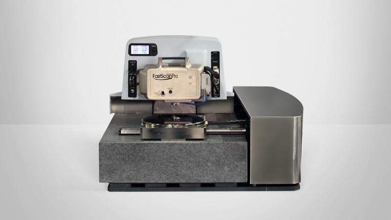
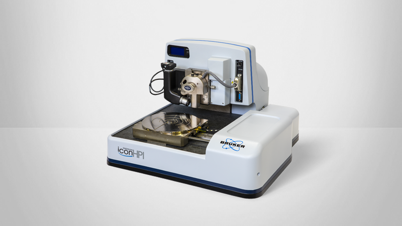
The Dimension® family of Atomic Force Microscopes (AFMs) have a long-standing reputation for providing the highest available speed and performance for industrial metrology applications. Designed specifically for high-volume, production environments, Dimension HPI and PRO systems enable automated measurements of many AFM modes while ensuring the utmost ease of use and the lowest cost per measurement for quality control, quality assurance, and failure analysis. Using contact, tapping, and PeakForce Tapping® mode techniques, these systems enable users to precisely control probe-to-sample interaction, providing long tip life-times with high-accuracy results in thousands of measurements.

Watch Our AFM Webinars
Our webinars cover best practices, introduce new products, provide quick solutions to tricky questions, and offer ideas for new applications, modes, or techniques.


How Can We Help?

Bruker partners with our customers to solve real-world application issues. We develop next-generation technologies and help customers select the right system and accessories. This partnership continues through training and extended service, long after the tools are sold.
Our highly trained team of support engineers, application scientists and subject-matter experts are wholly dedicated to maximizing your productivity with system service and upgrades, as well as application support and training.