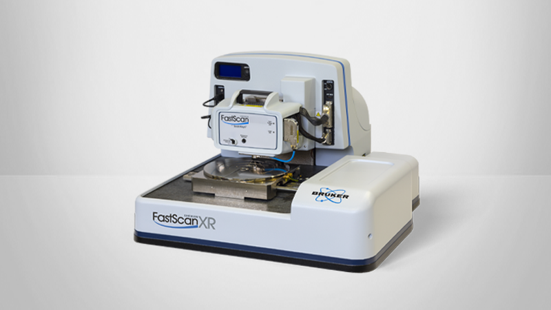
Scanning Microwave Impedance Microscopy (sMIM)
Complete Characterization of Complex Impedance for Nanoelectrical Devices
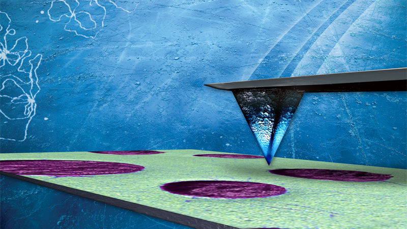
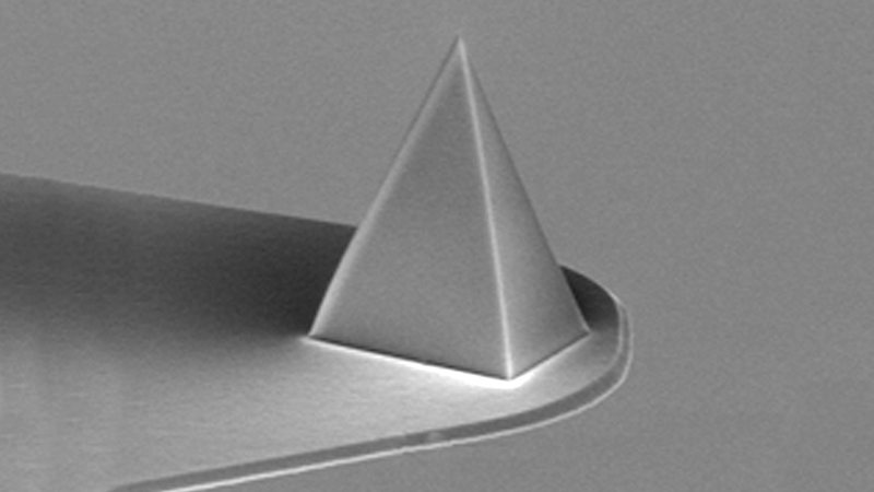
Scanning Microwave Impedance Microscopy (sMIM) uses a microwave signal that is reflected from the tip-sample interface to elucidate the electrodynamic properties of the sample surface underneath the tip apex. Detecting and processing the reflectance in real-time allows sMIM to directly access the permittivity and conductivity of the material. The near-field nature of sMIM, together with specialized AFM probes, delivers sub-aF sensitivity and allows routine electrical mapping with <30nm lateral resolution.
Bruker enhanced sMIM capabilities even further with the development of PeakForce sMIM and DataCube sMIM modes. These advanced sMIM modes provide simultaneous measurement of local variations in permittivity (ε) and conductivity (σ) for all types of materials relevant to nanoelectrical devices — including semiconductors, dielectrics, metals, metal oxides, buried structures, ferroelectrics, 1D and 2D materials, etc.
- PeakForce sMIM unlocks challenging applications, such as delicate and rough samples, and allows direct correlation to nanomechanical properties;
- DataCube sMIM enables hyperspectral mapping of sample impedance and ensures measurement repeatability; and
- sMIM with ScanWave Pro Solutions allows quantification of both carrier type and carrier concentration for doped semiconductors.

PeakForce sMIM
PeakForce sMIM couples sMIM with Bruker’s PeakForce Tapping® technology to greatly expand its application to previously challenging samples (e.g., carbon nanotubes, nanoparticle oxide films, and semiconductor devices) and provides simultaneous mapping of correlated nanomechanical properties.
PeakForce sMIM mode:
- Eliminates high-shear forces associated with contact-based electrical modes that can distort or dislocate delicate samples;
- Allows high-resolution imaging of rough sample surfaces and delivers highly sensitive electrical measurements by removing convolution from topographical data; and
- Enables multiparametric imaging with direct correlation to nanomechanical properties, such as modulus and adhesion.

DataCube sMIM
Bruker’s DataCube Modes extend the capabilities of sMIM to acquire multidimensional datasets.
DataCube sMIM mode:
- Enables voltage cycling at each pixel to provide a more comprehensive measurement of sample impedance in a single scan;
- Allows measurement and subtraction of background capacitance contributions, improving data acquisition sensitivity;
- Delivers correlated hyperspectral maps of nanoelectrical and nanomechanical properties; and
- Provides increased tip and sample lifetime for enhanced measurement repeatability.

ScanWave Pro Solutions
PrimeNano Inc. (the developer of sMIM) has now introduced ScanWave Pro Solutions for high-resolution quantitative carrier profiling of doped semiconductors, which
- Enables automated quantification of dopant levels and identification of dopant type (n-type or p-type);
- Provides highly repeatable measurements and highest sensitivity to dopant levels in the industry; and
- Is only available on Bruker’s Dimension Icon® SPMs.